System and Method for Direct Writing to a Wafer

a direct writing and wafer technology, applied in the field of semiconductor manufacturing, can solve the problems of time-consuming and labor-intensive exposing an entire wafer, and the cost of owning and operating a dw exposure tool

Active Publication Date: 2009-10-29
TAIWAN SEMICON MFG CO LTD
View PDF12 Cites 30 Cited by
  • Summary
  • Abstract
  • Description
  • Claims
  • Application Information

AI Technical Summary

Benefits of technology

[0004]More recent lithography-type systems for micro fabrication operate to transfer or generate an exposure pattern in a resist layer without the intermediary step of creating a photomask. For example, a direct-write (DW) exposure tool operates to write patterns directly into one or more layers on a substrate (without a photomask or reticle). The pattern is generally written from an electronic or computer-type file that is used to control a precision exposure source that may be selectively directed onto the layers of the substrate. More particularly, a DW exposure tool is generally configured such that the exposure of a circuit pattern is made not by illumination of the photo-resist through a mask or film negative of the circuit, but rather by directly and selectively exposing the desired areas of the resist or other layer on a substrate with a focused beam of the appropriate energy and dosage to create the desired circuit pattern. However, the DW exposure tool is expensive to own and operate, and exposing an entire wafer is time consuming. Accordingly, wafer throughput is low as compared to photolithography or other projection imaging systems.

Problems solved by technology

However, the DW exposure tool is expensive to own and operate, and exposing an entire wafer is time consuming.

Method used


Image

  • System and Method for Direct Writing to a Wafer
  • System and Method for Direct Writing to a Wafer
  • System and Method for Direct Writing to a Wafer

Examples


Embodiment Construction

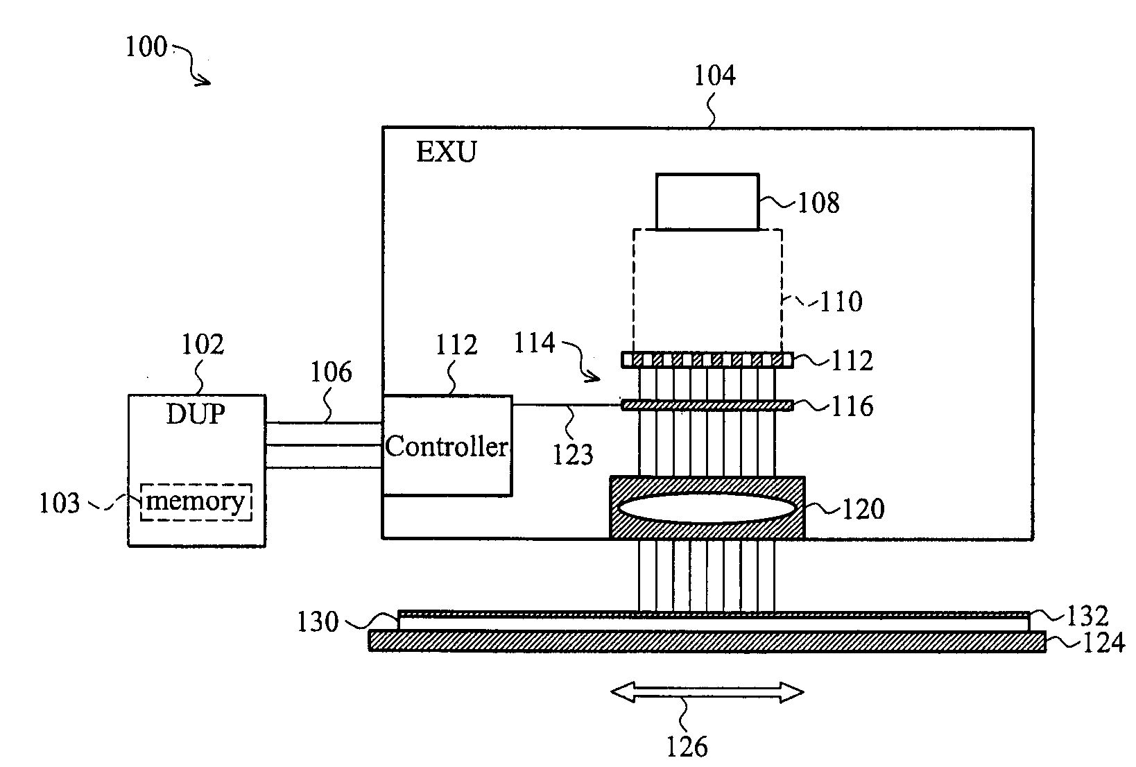
[0019]The present disclosure relates generally to semiconductor manufacturing and more particularly, to a system and method for writing directly to a wafer. It is understood, however, that specific embodiments are provided as examples to teach the broader inventive concept, and one of ordinary skill in the art can easily apply the teaching of the present disclosure to other methods or devices. In addition, it is understood that the methods and system discussed in the present disclosure include some conventional structures and / or processes. Since these structures and processes are well known in the art, they will only be discussed in a general level of detail. Furthermore, reference numbers are repeated throughout the drawings for sake of convenience and example, and such repetition does not indicate any required combination of features or steps throughout the drawings.

[0020]Referring to FIG. 1, illustrated is a diagrammatic view of an exemplary direct-write (DW) system 100. The DW s...


PUM


Abstract

A direct-write (DW) exposure system is provided which includes a stage for holding a substrate and configured to scan the substrate along an axis during exposure, a data processing module for processing pattering data and generating instructions associated with the patterning data, and an exposure module that includes a plurality of beams that are focused onto the substrate such that the beams cover a width that is larger than a width of a field size and a beam controller that controls the plurality of beams in accordance with the instructions as the substrate is scanned along the axis. The widths are in a direction different from the axis.

Description

PRIORITY DATA[0001]This application claims priority to Provisional Application Ser. No. 61 / 047,931, filed on Apr. 25, 2008, entitled “SYSTEM AND METHOD FOR DIRECT WRITING TO A WAFER, the entire disclosure of which is incorporated herein by reference.BACKGROUND[0002]The present disclosure relates generally to semiconductor manufacturing and, more particularly, to a system and method for direct writing to a wafer.[0003]Photolithography or optical lithography is generally known as a process that is used in micro fabrication to selectively remove parts of thin films on a substrate. Photolithography generally uses a directed light source to transfer a geometric pattern from a photomask to a light-sensitive chemical resist material that is formed on the substrate, thus generating an exposure pattern in the resist material from the light radiation. A series of chemical treatments may then be used to etch or otherwise transfer the exposure pattern into one or more thin film layers positione...

Claims


Application Information

Patent Timeline
Patent Type & Authority Applications(United States)
IPC IPC(8): G03B27/54
CPCB82Y10/00H01J37/3174G03F7/70383B82Y40/00
Inventor LIN, BURN JENGCHEN, JENG-HORNGLIN, SHY-JAYGAU, TSAI-SHENG
Owner TAIWAN SEMICON MFG CO LTD
Why Eureka
Try Eureka