ZnO BASED SEMICONDUCTOR LIGHT EMITTING DEVICE AND ITS MANUFACTURE METHOD

Active Publication Date: 2009-11-05
STANLEY ELECTRIC CO LTD
View PDF4 Cites 2 Cited by
  • Summary
  • Abstract
  • Description
  • Claims
  • Application Information

AI Technical Summary

Benefits of technology

[0011]It is an object of the present invention to provide a ZnO based semiconductor light emitting device with an improved emission efficiency using a ZnO1-xSx emission layer, and a manufacture method for such a semiconductor light emitting device.

Problems solved by technology

However, since Cd is a highly toxic element, adopting ZnCdO mixed crystal is difficult from the viewpoint of safety.

Method used


Image

  • ZnO BASED SEMICONDUCTOR LIGHT EMITTING DEVICE AND ITS MANUFACTURE METHOD
  • ZnO BASED SEMICONDUCTOR LIGHT EMITTING DEVICE AND ITS MANUFACTURE METHOD
  • ZnO BASED SEMICONDUCTOR LIGHT EMITTING DEVICE AND ITS MANUFACTURE METHOD

Examples


first embodiment

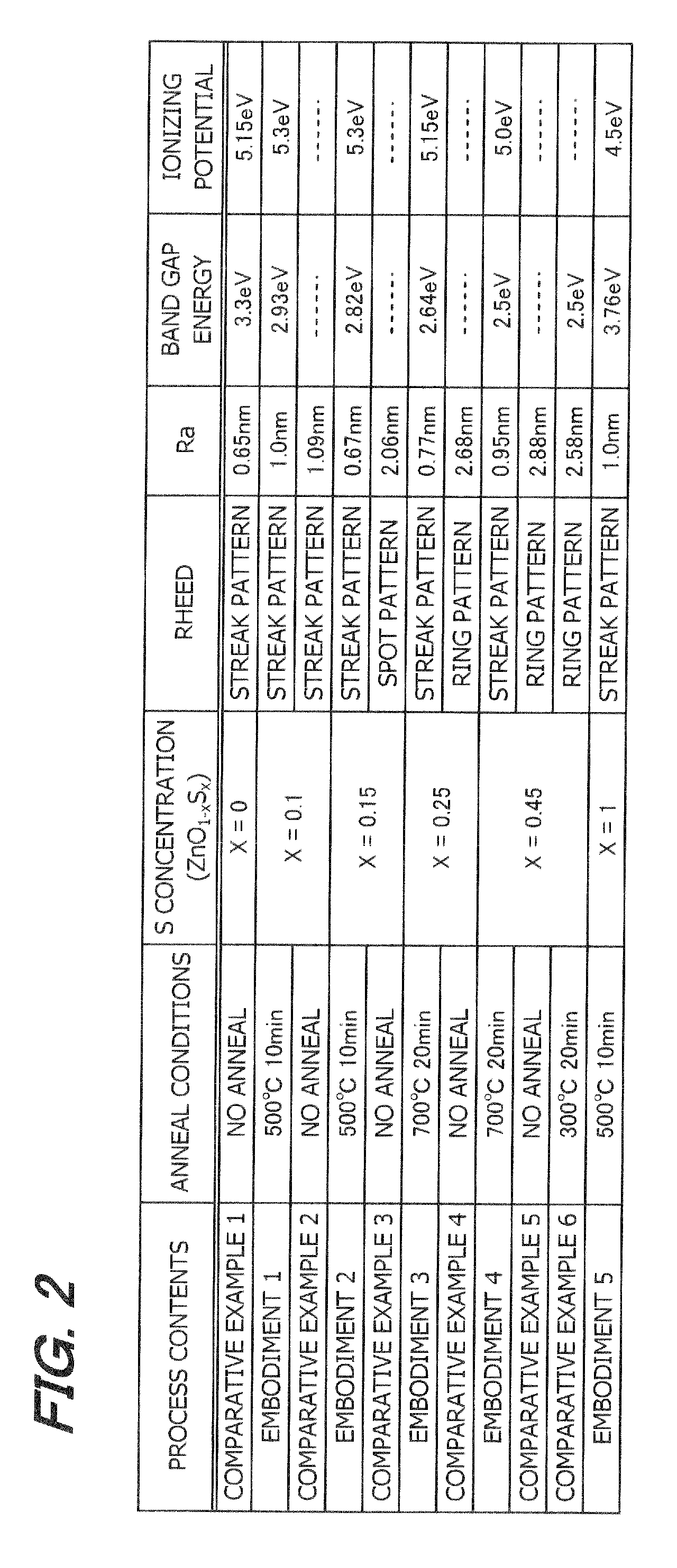
[0041]Evaluation results by the above-described method indicated that the ZnO1-xSx layer of the first embodiment had an S composition x of 0.1, a band gap energy was 2.93 eV, a surface roughness Ra was 1.0 nm, and an ionizing potential was 5.3 eV. An RHEED image of the ZnO1-xSx layer of the thin sample had a streak pattern. The ZnO1-xSx layer having good crystallinity and flatness was obtained.

[0042]Next, the second comparative example will be described. A ZnO1-xSx layer was grown to a thickness of 100 nm by the method similar to the first embodiment. As different from the first embodiment, annealing was not performed after the film was formed.

[0043]A surface roughness was measured with AFM, and RHEED measurements were conducted during growth. The ZnO1-xSx layer of the second comparative example had a surface roughness Ra of 1.09 nm, and the RHEED image indicated a streak pattern. Since an S concentration is low, it can be considered that a film having relatively good crystallinity ...

seventh embodiment

[0101]After these electrodes are formed, an electrode alloying process is performed, for example, in an oxygen atmosphere at 400° C. to 800° C. An alloying process time is, for example, one minute to ten minutes. In this manner, the light emitting device of the seventh embodiment is manufactured. Although the ZnO substrate having n-type conductivity is used as the substrate 8, an SiC substrate and a GaN substrate having n-type conductivity may also be used.

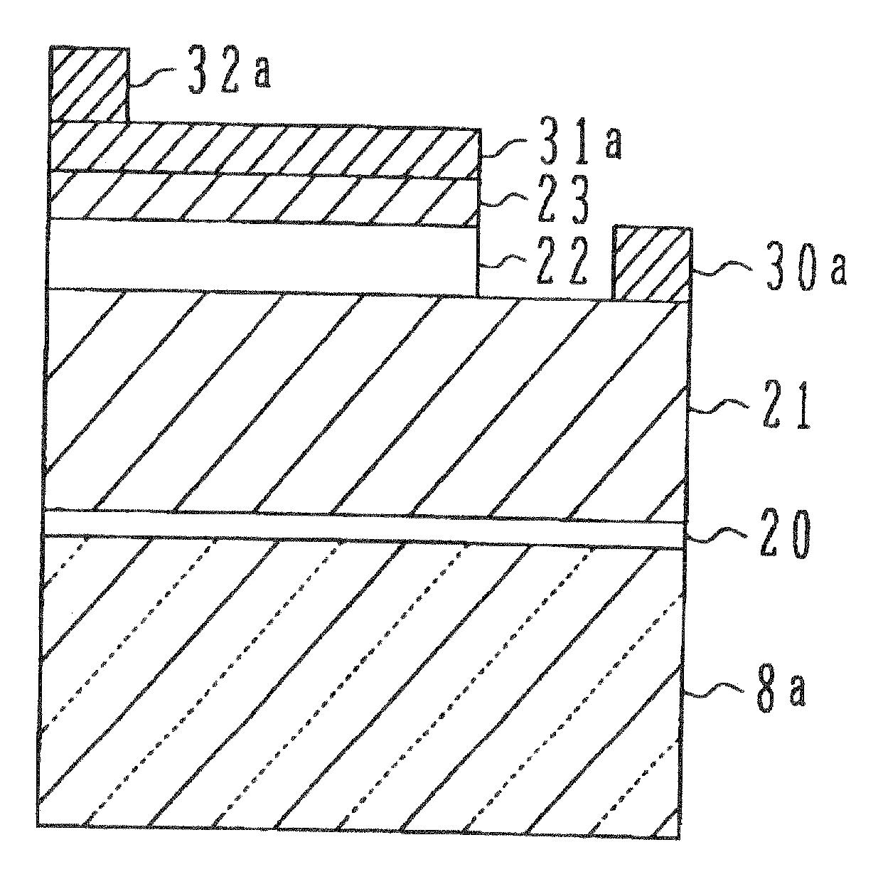
[0102]Next, with reference to FIG. 10, description will be made on a manufacture method for a light emitting device of the eighth embodiment. Different points from the seventh embodiment reside in that an insulating sapphire substrate 8a is used and therefore an electrode forming process is changed.

[0103]Similar to the seventh embodiment, layers from an n-type ZnO buffer layer 20 to a p-type ZnO layer 23 are formed on the substrate 8a. After the wafer formed with the layers up to the p-type ZnO layer 23 is dismounted from the film...

eighth embodiment

[0107]In the light emitting device of the eighth embodiment, the insulating sapphire substrate can be used. A ZnO substrate, an SiC substrate or a GaN substrate may also be used.

[0108]In the above-described embodiments, the c-plane ZnO substrate is used and the semiconductor device is formed on the + c-plane by way of example. The semiconductor device may be formed on the − c-plane. The semiconductor device may be formed also on the ZnO substrate having the a-plane or an m-plane.

[0109]As described above, setting 0.251-xSx layer is sandwiched between ZnO layers, carriers can be confined in the ZnO1-xSx layer. It is therefore expected for example that a blue light emitting device having a high emission efficiency can be manufactured. By performing annealing at 500° C. or higher, and lower than 1000° C. after the ZnO1-xSx layer is formed, flatness of the ZnO1-xSx layer can be improved.

[0110]As studies have been made with reference to FIG. 4, the structure that the ZnO1-xSx layer is san...


PUM


Abstract

A ZnO based semiconductor light emitting device includes: a first semiconductor layer containing ZnO1-x1Sx1; a second semiconductor layer formed above the first semiconductor layer and containing ZnO1-x2Sx2; and a third semiconductor layer formed above the second semiconductor layer and containing ZnO1-x3Sx3, wherein an S composition x1 of the first semiconductor layer, an S composition x2 of the second semiconductor layer and an S composition x3 of the third semiconductor layer are so selected that an energy of the second semiconductor layer at the lower end of a conduction band becomes lower than both energies of the first and third semiconductor layers at the lower end of the conduction bands, and that an energy of the second semiconductor layer at the upper end of a valence band becomes higher than both energies of the first and third semiconductor layers at the upper end of the valence bands.

Description

CROSS REFERENCE TO RELATED APPLICATION[0001]This application is a continuation application of PCT / JP2008 / 000019, filed on Jan. 11, 2008, the entire contents of which are incorporated herein by reference.BACKGROUND OF THE INVENTION[0002]A) Field of the Invention[0003]The present invention relates to a ZnO based semiconductor light emitting device and its manufacture method.[0004]B) Description of the Related Art[0005]A transition energy between bands of zinc oxide (ZnO) corresponds to an emission energy in a ultraviolet range of about 370 nm. This wavelength is shorter than a visual light range of 400 nm or longer providing a high industrial usage value. In order to obtain emission at a wavelength longer than 400 nm, studies have been made to narrow a band gap (gap narrowing) of ZnO.[0006]As the gap narrowing techniques of narrowing a band gap of ZnO, ZnCdO mixed crystal replacing a portion of Zn with Cd has been proposed in which the band gap can be adjusted in a range of 3.4 eV to ...

Claims


Application Information

Patent Timeline
IPC IPC(8): H01L33/00H01L33/28
CPCH01L21/0237H01L21/02403H01L21/02433H01L21/02472H01L33/28H01L21/02557H01L21/02609H01L21/02631H01L21/02554
Inventor OGAWA, AKIOSANO, MICHIHIROKATO, HIROYUKIKOTANI, HIROSHIYAMAMURO, TOMOFUMI
Owner STANLEY ELECTRIC CO LTD
Why Eureka
Try Eureka