Plasmostor: a-metal-oxide-si field effect plasmonic modulator

a plasmonic modulator and metal oxide technology, applied in the field of optical modulators, can solve the problems of accompanied mos scaling, increased circuit delay, and higher electronic power dissipation

Inactive Publication Date: 2009-11-05
CALIFORNIA INST OF TECH
View PDF2 Cites 32 Cited by
  • Summary
  • Abstract
  • Description
  • Claims
  • Application Information

AI Technical Summary

Problems solved by technology

Unfortunately, as gate lengths approach dimensions measured in single nanometers, MOS scaling is accompanied by increased circuit delay and higher electronic power dissipation.
This is a substantial problem for Moore's Law which often referred to as the “interconnect bottleneck.”
Unfortunately, optical components are generally bulky relative to CMOS electronic devices, comprising dimensions on the order of the signal wavelength.

Method used


Image

  • Plasmostor:  a-metal-oxide-si field effect plasmonic modulator
  • Plasmostor:  a-metal-oxide-si field effect plasmonic modulator
  • Plasmostor:  a-metal-oxide-si field effect plasmonic modulator

Examples


Embodiment Construction

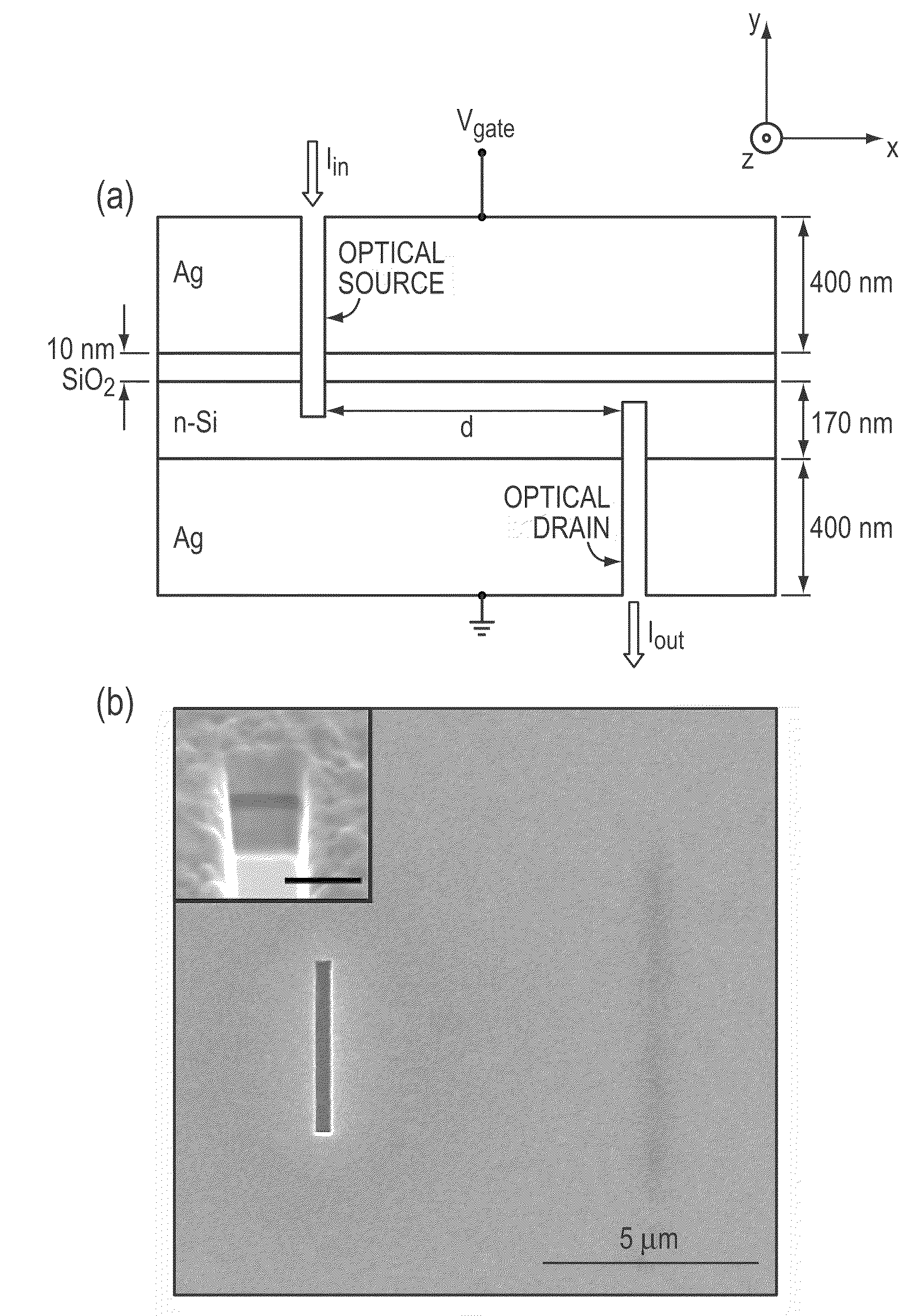
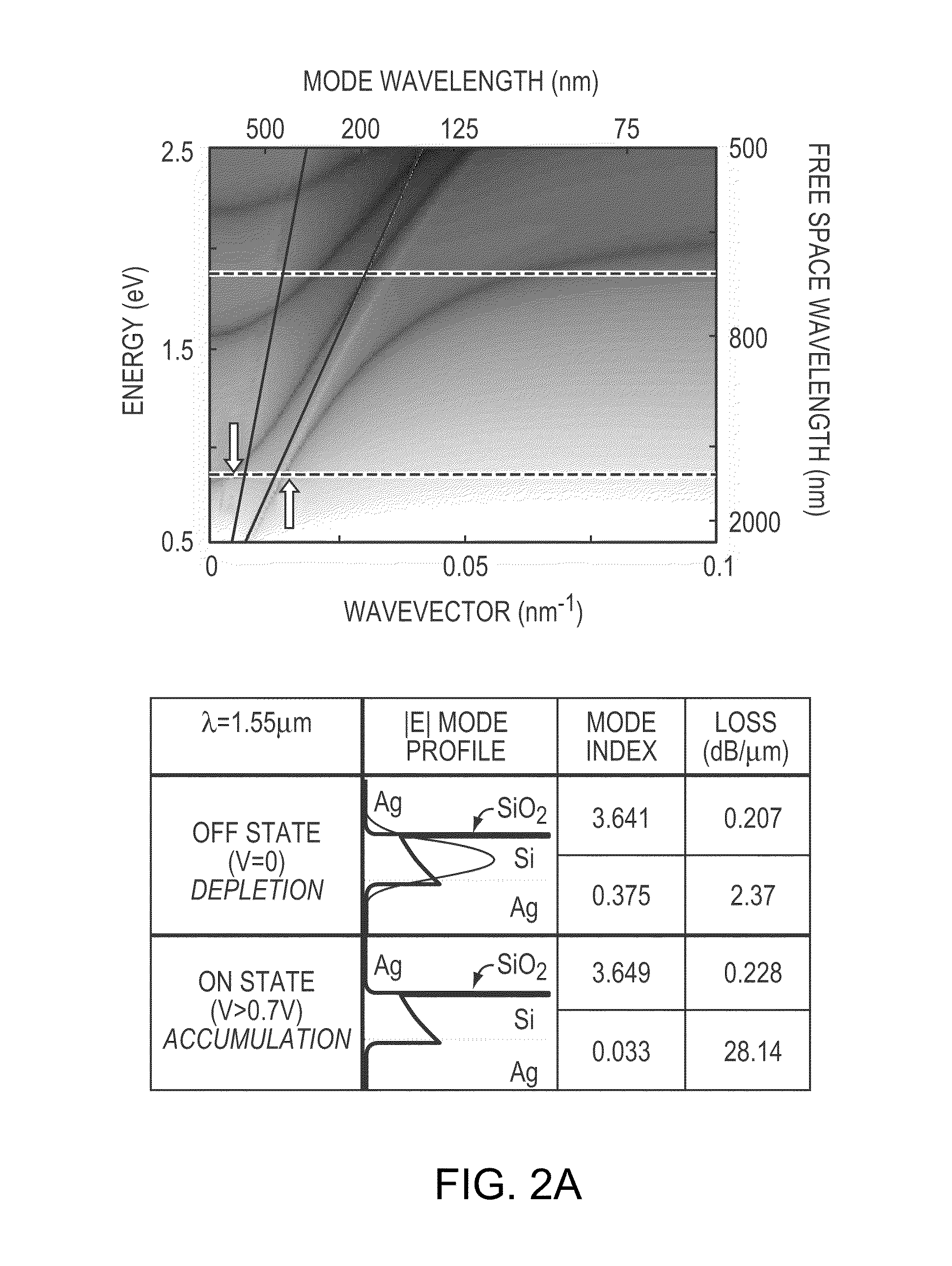
[0035]Ultracompact silicon-compatible modulators, ideally comprising dimensions, materials, and functionality similar to electronic complementary metal-oxide-semiconductor (CMOS) components are expected to be useful to provide chip-based all-optical and optoelectronic computational networks. We have demonstrated such a modulator, based on field-effect modulation of plasmon waveguide modes in a MOS geometry. Near-infrared transmission between an optical source and drain is controlled by a gate voltage that drives the MOS into accumulation. Using the gate oxide as an optical channel, electro-optic modulation is achieved in device volumes of half of a cubic wavelength with femtoJoule switching energies and the potential for GHz modulation frequencies. Modulation has been observed in devices with channel areas (length×thickness) as small as 0.01λ2, with sub-nanosecond switching speeds.

[0036]We present a demonstration of a field effect Si modulator based on multimode interferometry in a ...


PUM

PropertyMeasurementUnit
wavelengthaaaaaaaaaa

Abstract

The invention is a system and method for performing all-optical modulation. A semiconductor layer having a defined thickness has an insulator adjacent one surface of the semiconductor. Conductive layers are provided adjacent the semiconductor layer and the insulator. A photodetector is provided to generate an electric field across the conductive layers in response to an input optical gate signal. An input optical signal is modulated by interaction with a plasmon wave generated at the semiconductor / conductive layer interface. By defining the thickness of the semiconductor layer, a desired wavelength of light supports the plasmon waves. Operation of the all-optical modulator requires the provision of an input optical signal of a desired wavelength and the provision of a gate optical signal. An output optical signal is recovered and can be used to store, display or transmit information, for example over a fiber optic communication system, such as a telecommunication system.

Description

CROSS-REFERENCE TO RELATED APPLICATIONS[0001]This application claims priority to and the benefit of co-pending U.S. provisional patent application Ser. No. 61 / 070,523, filed Mar. 24, 2008, and co-pending U.S. provisional patent application Ser. No. 61 / 132,831, filed Jun. 23, 2008, each of which applications is incorporated herein by reference in its entirety.STATEMENT REGARDING FEDERALLY FUNDED RESEARCH OR DEVELOPMENT[0002]The U.S. Government has certain rights in this invention pursuant to Grant No. FA9550-04-1-0434 awarded by the Air Force Office of Scientific Research (AFOSR).THE NAMES OF THE PARTIES TO A JOINT RESEARCH AGREEMENT[0003]Not Applicable.INCORPORATION-BY-REFERENCE OF MATERIAL SUBMITTED ON A COMPACT DISC[0004]Not Applicable.BACKGROUND OF THE INVENTION[0005]1. Field of the Invention[0006]The invention relates to optical modulators in general and particularly to an optical modulator that employs silicon (Si) as an active medium in a plasmonic device.[0007]2. Description ...

Claims


Application Information

Patent Timeline
Patent Type & Authority Applications(United States)
IPC IPC(8): G06E3/00G02F1/00
CPCG02F2203/10G02F1/025
Inventor DIONNE, JENNIFER A.DIEST, KENNETH A.SWEATLOCK, LUKEATWATER, HARRY A.
Owner CALIFORNIA INST OF TECH
Why Eureka
Try Eureka