Calibration of non-vibrating contact potential difference measurements to detect surface variations that are perpendicular to the direction of sensor motion

Inactive Publication Date: 2009-11-05
QCEPT INVESTMENTS LLC
View PDF78 Cites 6 Cited by
  • Summary
  • Abstract
  • Description
  • Claims
  • Application Information

AI Technical Summary

Benefits of technology

[0013]The system and methods described in this invention provide an enhanced application of a combined vibrating and non-vibrating contact potential difference inspection system that allows the rapid imaging of surfaces and the detection of surface potential non-uniformities in both the direction of motion of the non-vibrating (scanning) probe and perpendicular to the direction of motion of the non-vibrating probe. This capability is particularly useful for the detection of radial non-uniformities on surfaces scanned with a non-vibrating probe using a radial scanning system. Hereinafter, material susceptible to inspection by the system herein described will be denoted generally as a “wafer”. In preferred applications, such as for evaluation of conventional silicon single crystal wafers, various examples are described hereinafter for four different wafers subjected to different processing conditions. The invention includes both a vibrating and a non-vibrating contact potential difference measurement capability. The vibrating contact pot

Problems solved by technology

Also, the sensor output does not provide data on the absolute contact potential difference between the probe tip and measured surface at any point.
The integrated signal provides information on relative surface potentials in the direction of motion of the probe, but does not provide any information about surface variations perpendicular to the direction of motion, nor does it provide a measure of the absolute value of the contact potential difference.
However, this operation requires two scans of the surface, which doubles the scanning time.
In the case of radial scanning, the scanning mechanics do not easily lend themselves to scanning each point on the wafer surface in two orthogonal directions.
As a result, the circular motion of the probe relative to the wafer su

Method used


Image

  • Calibration of non-vibrating contact potential difference measurements to detect surface variations that are perpendicular to the direction of sensor motion
  • Calibration of non-vibrating contact potential difference measurements to detect surface variations that are perpendicular to the direction of sensor motion
  • Calibration of non-vibrating contact potential difference measurements to detect surface variations that are perpendicular to the direction of sensor motion

Examples


Example

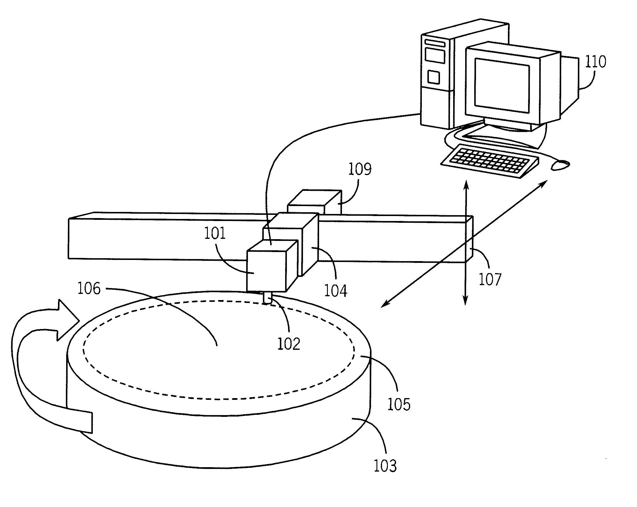
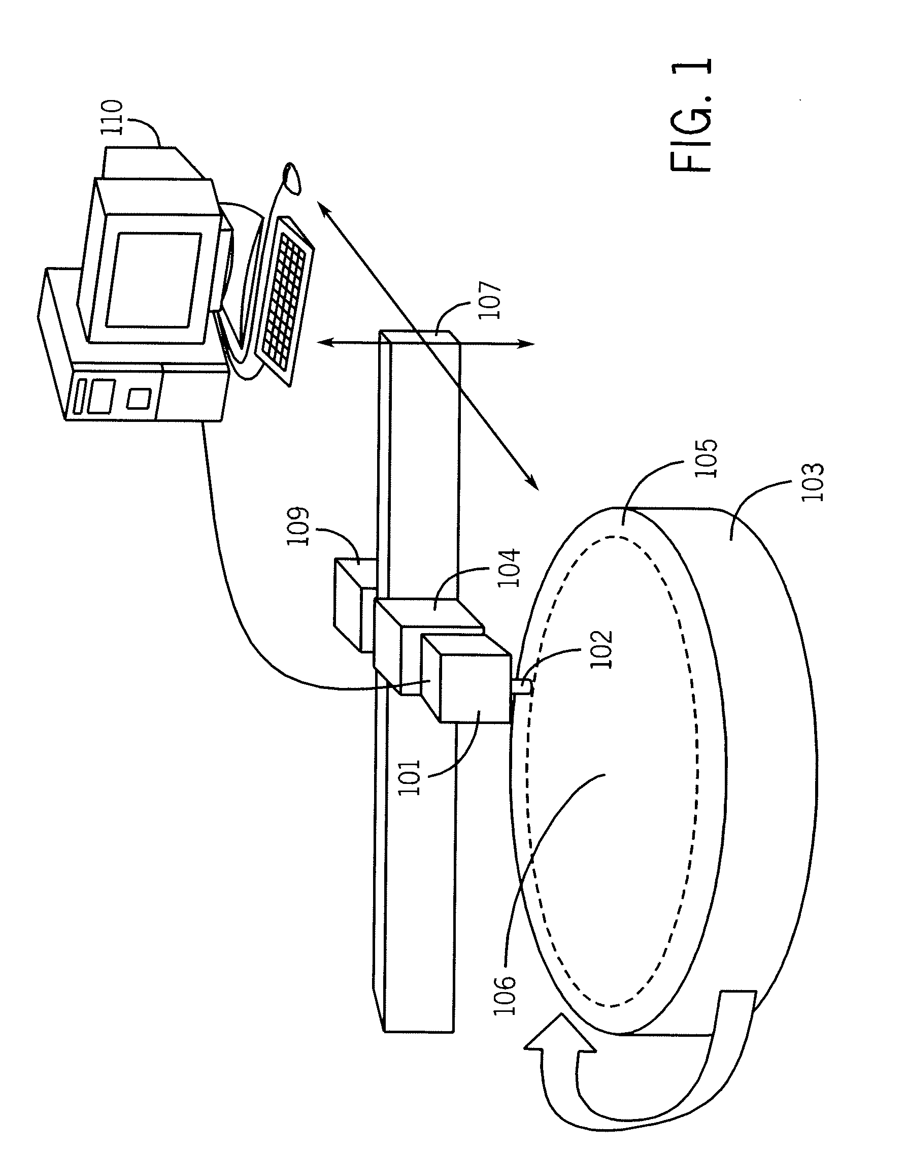
[0051]In accordance with one preferred embodiment, a radial scanning apparatus 100 is shown in FIG. 1. The apparatus 100 consists of a contact potential difference sensor 101, a system 103 for mechanically fixturing wafer 105 and spinning the wafer 105 to generate relative motion between probe tip 102 and wafer surface 106 such that the probe tip 102 moves parallel to the wafer surface 106, a system 107 for positioning the sensor 101 a fixed distance above the wafer surface 106, a system 104 for vibrating the probe tip perpendicular to the wafer surface, and a system 110 for acquiring and processing the output signal from the sensor 101 to identify and classify wafer 105 non-uniformities. In this preferred embodiment, the contact potential difference sensor 101 can be operated as a non-vibrating contact potential difference sensor to scan the wafer surface 106 and generate data on changes in contact potential difference across the wafer surface 106, or as a vibrating contact potenti...


PUM


Abstract

A method and system for determining the contact potential difference of a wafer surface using a non-vibrating contact potential difference probe and a vibrating contact potential difference probe. The method and system involves scanning the wafer surface with a non-vibrating contact potential difference sensor, integrating and scaling the resulting data, and applying offsets to individual tracks of data to match the integrated scaled data to measurements made using a vibrating contact potential difference sensor.

Description

[0001]The present invention is directed to methods and systems for the inspection of surfaces and materials, including semiconductor surfaces and semiconductor materials. More particularly, the present invention is directed to methods for detecting and measuring surface or subsurface non-uniformities and / or charges using contact potential difference sensors in both vibrating and non-vibrating modes so as to establish the presence of any non-uniformities with precision over the entire surface.BACKGROUND OF THE INVENTION[0002]The function, reliability and performance of semiconductor devices depend on the use of semiconductor materials and surfaces which are clean and uniform. Billions of dollars and countless man-hours have been spent developing, characterizing, and optimizing systems and processes for fabricating and processing semiconductor materials. A primary goal of this activity has been the fabrication of materials and surfaces that are extremely clean and that have predetermi...

Claims


Application Information

Patent Timeline
IPC IPC(8): G01D21/00
CPCH01L22/14G01N27/002
Inventor SCHULZE, MARK A.USRY, WILLIAM R.
Owner QCEPT INVESTMENTS LLC
Why Eureka
Try Eureka