Method of manufacturing inkjet printhead and inkjet printhead manufactured using the same
a technology of inkjet printing and inkjet printing, which is applied in the direction of printing, metal-working equipment, writing implements, etc., can solve problems such as cracks in the nozzle layer, and achieve the effect of preventing or substantially reducing nozzle cracks and image quality deterioration
- Summary
- Abstract
- Description
- Claims
- Application Information
AI Technical Summary
Benefits of technology
Problems solved by technology
Method used
Image
Examples
preparation example 1
Preparation of Negative Photoresist Composition
[0110]30 gram (g) of Propylene Glycol Methyl Ether Acetate (PGMEA) (Samchun Chemical Co.), 2 g of diglycidyl hexahydro phthalate (Sigma-Aldrich Co.), and 2 g of SP-172 (Asahi Denka Korea Chemical Co.) were added to a jar in order to prepare a resist solution. Then, 40 g of EPON SU-8 (Hexion Speciality Co.) was then added thereto. The mixture was mixed in an impeller for 24 hours before being used to prepare a negative photoresist composition.
preparation example 2
[0111]A negative photoresist composition was prepared in the same manner as described in Preparation Example 1, except that the diglycidyl hexahydro phthalate was not used.
example 1
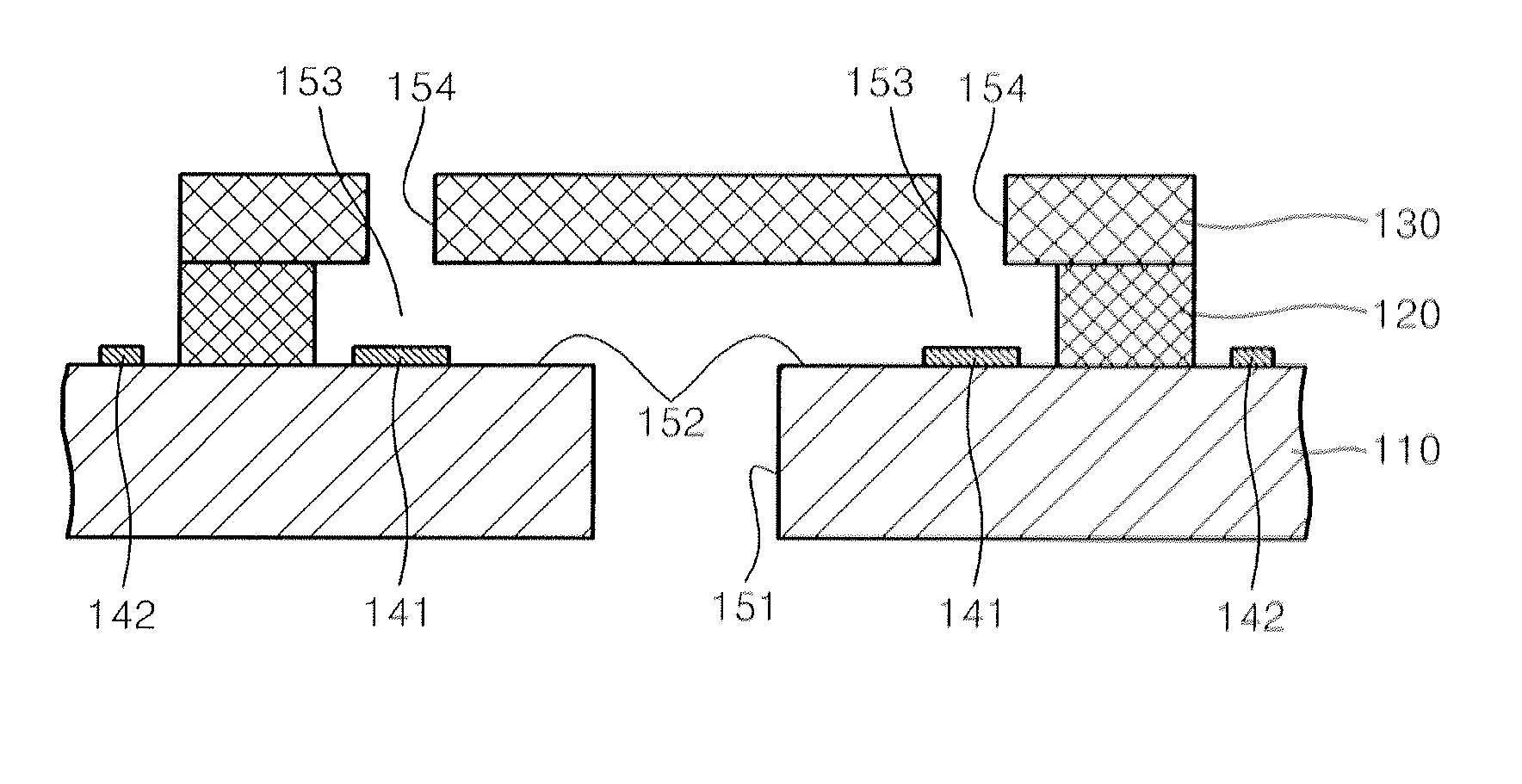
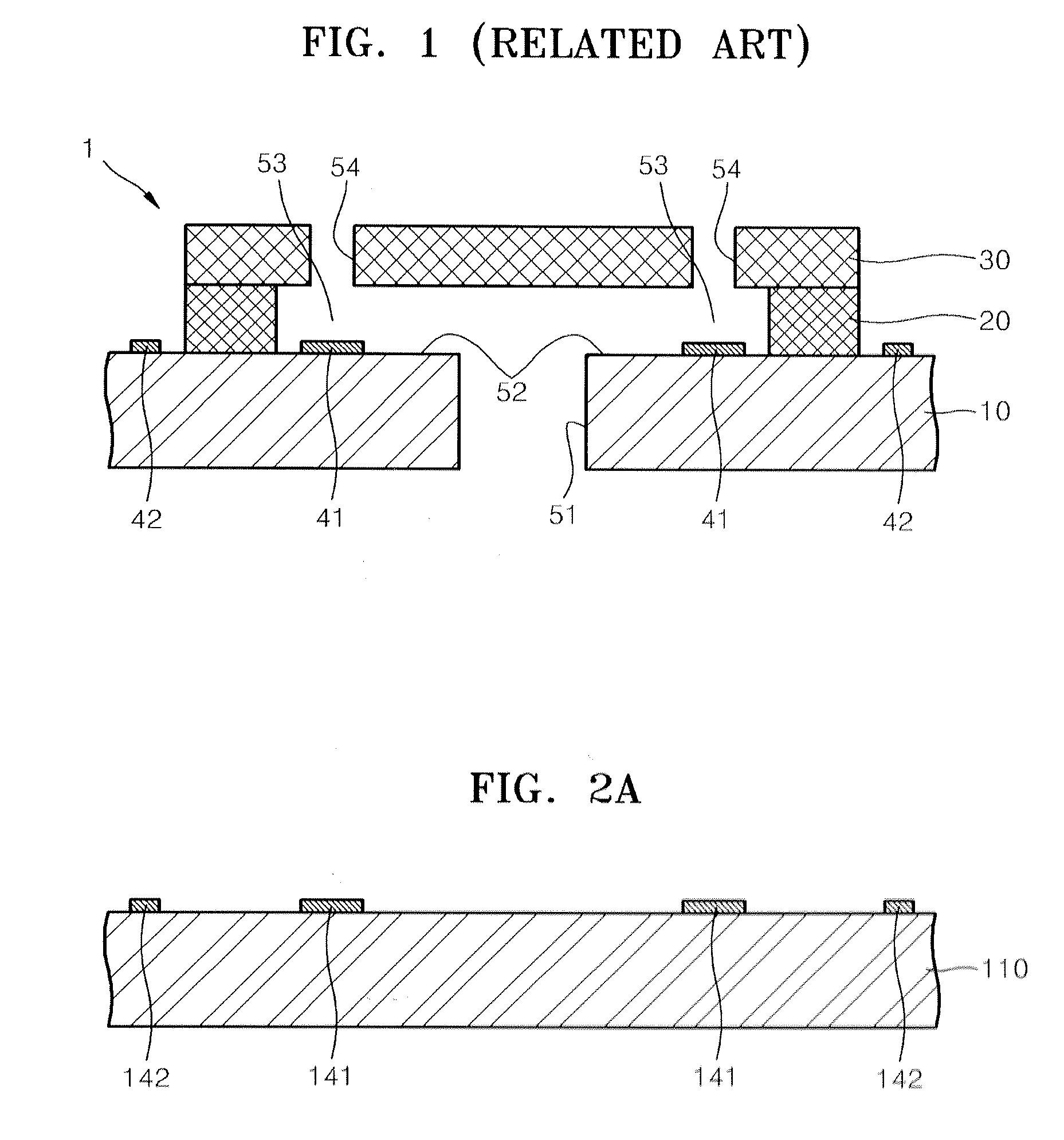
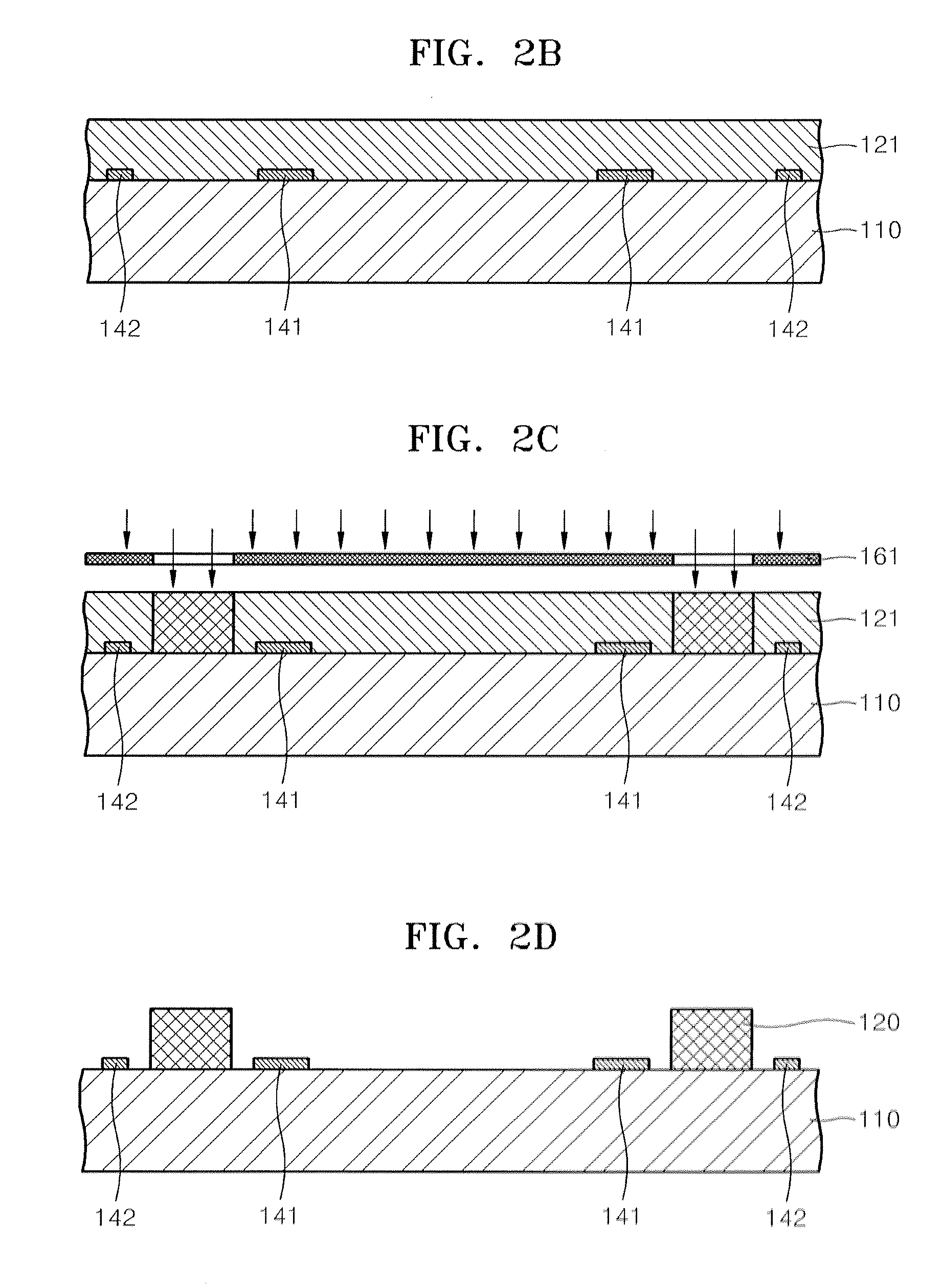
[0112]A tantalum nitride heater pattern 141 having a thickness of about 500 Å and an electrode pattern 142 which was formed of an aluminum silicon copper (AlSiCu) alloy (the amounts of Si and Cu are respectively less than 1 wt %) having a thickness of about 500 Å were formed on a 6-inch silicon wafer 110 by using a sputtering process and photolithography (FIG. 2A).
[0113]Then, as illustrated in FIG. 2B, a negative photoresist composition prepared according to Preparation Example 1 was spin coated on a front surface of the silicon wafer, on which the heater pattern and the electrode pattern are formed, at a rate of 2000 rpm for 40 seconds, and the resultant was then baked at 95° C. for 7 minutes in order to form a first negative photoresist layer having a thickness of about 10 μm. Then, as illustrated in FIG. 2C, the first negative photoresist layer was exposed to i-line UV rays by using a first photomask having a predetermined ink chamber pattern and restrictor pattern formed thereon...
PUM
| Property | Measurement | Unit |
|---|---|---|
| nozzle chamber angle | aaaaa | aaaaa |
| thickness | aaaaa | aaaaa |
| thickness | aaaaa | aaaaa |
Abstract
Description
Claims
Application Information


