Semiconductor device and manufacturing method of the same

a semiconductor and display technology, applied in the direction of transistors, optics, instruments, etc., can solve the problems of low voltage supply due to a voltage drop through the wiring resistance, difficult to supply normal voltage and current, and difficulty in normal display and operation

Active Publication Date: 2009-11-19
SEMICON ENERGY LAB CO LTD
View PDF99 Cites 218 Cited by
  • Summary
  • Abstract
  • Description
  • Claims
  • Application Information

AI Technical Summary

Benefits of technology

[0017]By employing such a structure, a light-transmitting transistor or a light-transmitting capacitor element can be formed. Therefore, even though the transistor or the capacitor element is provided in a pixel, a decrease in an aperture ratio can be suppressed. Further, since a wiring for connecting the transistor and an element (e.g., another transistor) or a wiring for connecting the capacitor element and an element (e.g., another capacitor element) is formed by using a material with low resistivity and high conductivity, the blunting of the waveform of a signal and a voltage drop due to wiring resistance can be suppressed.
[0020]Further in the conductive layers, a light-transmitting region (a region with high light transmittance) and a light-shielding region (a region with low light transmittance) can be formed by one mask (reticle) with use of a multi-tone mask. Accordingly, the light-transmitting region (the region with high light transmittance) and the light-shielding region (the region with low light transmittance) can be formed without increasing the number of masks.
[0022]According to one embodiment of this invention, the light-transmitting transistor or the light-transmitting capacitor element can be formed. Therefore, even if the transistor or the capacitor is provided in a pixel, aperture ratio can be made high. Further, since a wiring for connecting the transistor and an element (e.g., another transistor) or a wiring for connecting a capacitor element and an element (e.g., another capacitor element) can be formed by using a material with low resistivity and high conductivity, the distortion of the waveform of a signal and a voltage drop due to wiring resistance can be reduced.

Problems solved by technology

As wiring resistance increases, the waveform of a signal which is transmitted through the wiring becomes distorted, resulting in a low voltage supply due to a voltage drop through the wiring resistance.
Therefore, it is difficult to supply normal voltage and current, whereby normal display and operation become difficult.
However, since a light-shielding material is used for the gate electrode and the source and drain electrodes, aperture ratio decreases and power consumption becomes high.

Method used


Image

  • Semiconductor device and manufacturing method of the same
  • Semiconductor device and manufacturing method of the same
  • Semiconductor device and manufacturing method of the same

Examples


embodiment 1

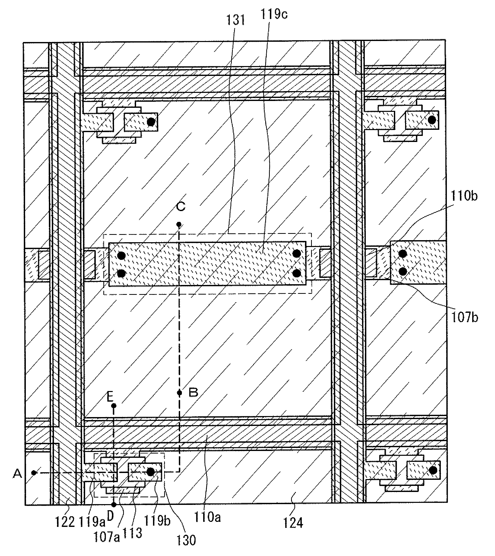
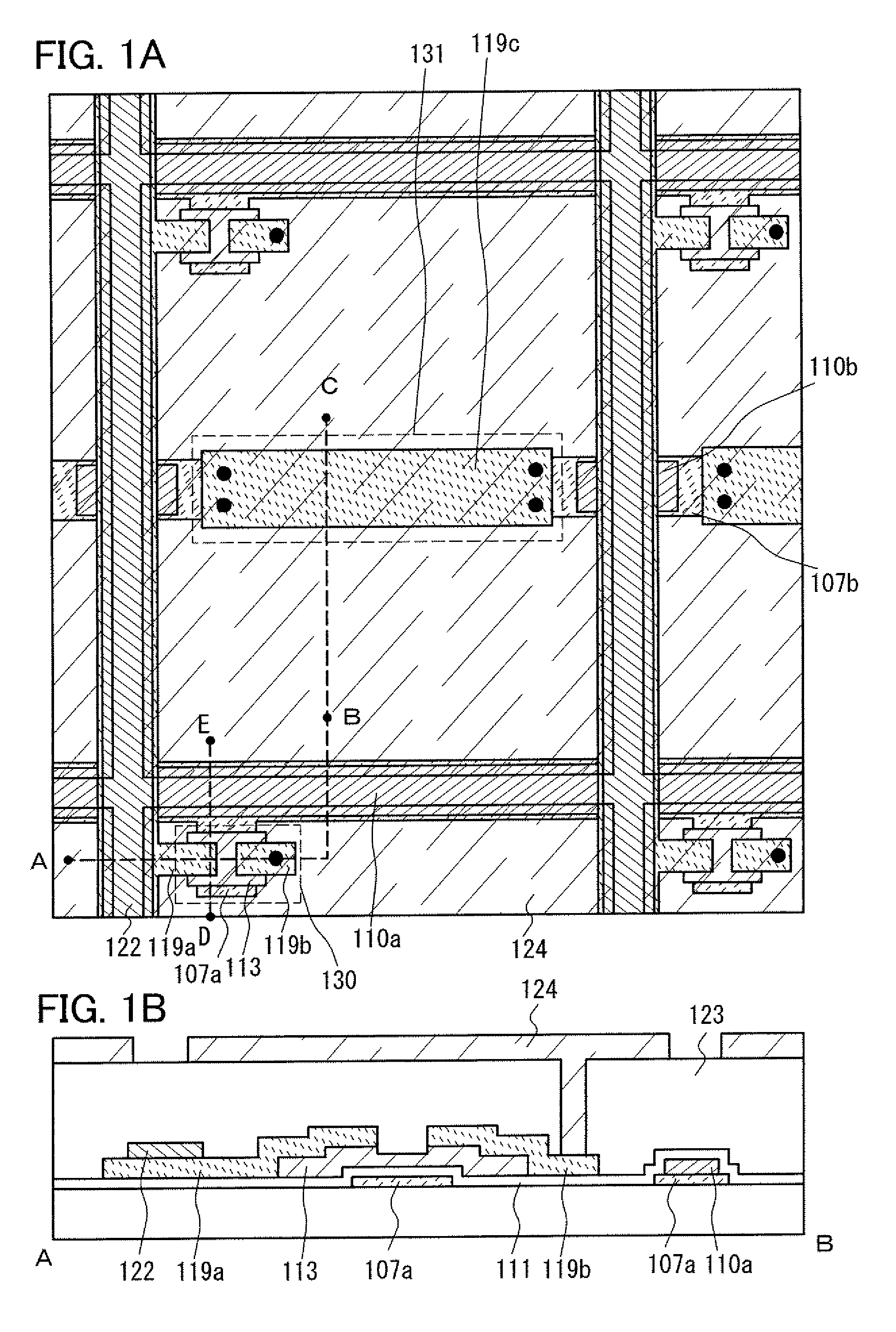
[0044]FIG. 1A is a top view illustrating one example of a semiconductor device of this embodiment and FIG. 1B is a cross-sectional view of FIG. 1A along line A-B.

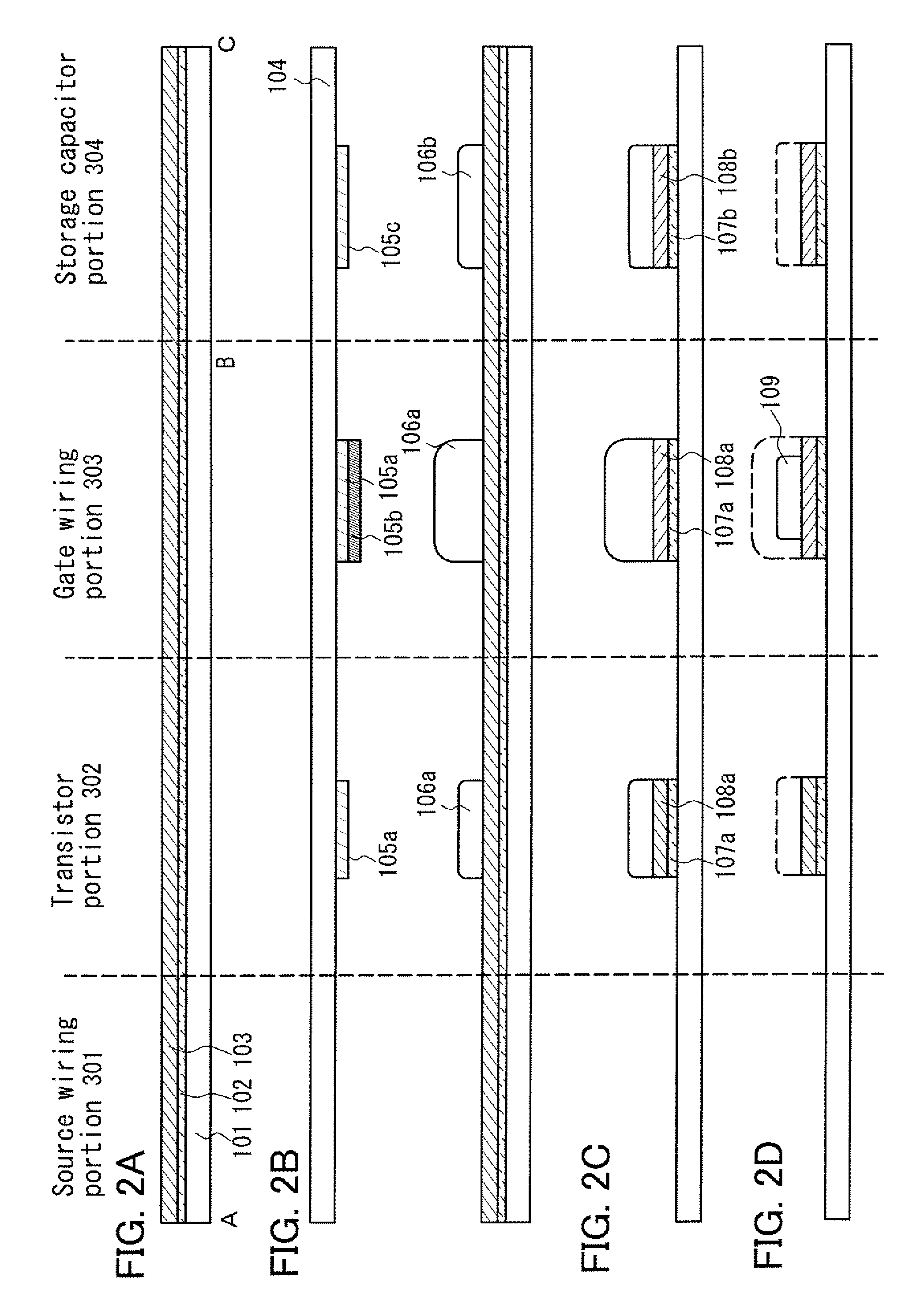
[0045]As shown in FIG. 1A, an element substrate includes a pixel portion which has a gate wiring and a storage capacitor line provided in direction 1, a source wiring provided in direction 2 which intersects with the gate wiring and the storage capacitor line, and a transistor around a portion where the gate wiring and the source wiring intersect with each other.

[0046]In order to increase the aperture ratio of a pixel, a transistor of this embodiment includes a light-transmitting conductive layer which functions as a gate electrode, a gate insulating film formed over the light-transmitting conductive layer, a semiconductor layer formed over the light-transmitting conductive layer which functions as the gate electrode with the gate insulating film interposed therebetween, and light-transmitting conductive layers which functi...

embodiment 2

[0177]An element substrate of one embodiment of this invention and a display device or the like including the element substrate can be used for an active matrix display panel. That is, one embodiment of the invention can be carried out in all electronic devices in which they are incorporated into a display portion.

[0178]Examples of such electronic devices include cameras such as a video camera and a digital camera, a head-mounted display (a goggle-type display), a car navigation system, a projector, a car stereo, a personal computer, and a portable information terminal (e.g., a mobile computer, a cellular phone, and an e-book reader). Examples of these devices are illustrated in FIGS. 15A to 15C.

[0179]FIG. 15A illustrates a television device. The television device can be completed by incorporating a display panel in a chassis, as illustrated in FIG. 15A. A main screen 2003 is formed using the display panel, and other accessories such as a speaker portion 2009 and an operation switch...


PUM

PropertyMeasurementUnit
transmittanceaaaaaaaaaa

Abstract

An object is to provide a semiconductor device with high aperture ratio or a manufacturing method thereof. Another object is to provide semiconductor device with low power consumption or a manufacturing method thereof. A light-transmitting conductive layer which functions as a gate electrode, a gate insulating film formed over the light-transmitting conductive layer, a semiconductor layer formed over the light-transmitting conductive layer which functions as the gate electrode with the gate insulating film interposed therebetween, and a light-transmitting conductive layer which is electrically connected to the semiconductor layer and functions as source and drain electrodes are included.

Description

BACKGROUND OF THE INVENTION[0001]1 Field of the Invention[0002]This invention relates to a semiconductor device, a display device, a producing method thereof, or a method using the semiconductor device or the display device. In specific, this invention relates to a semiconductor device and a display device each including a light-transmitting semiconductor layer, a producing method thereof, or a method using the semiconductor device or the display device. Further in specific, this invention relates to a liquid crystal display device including a light-transmitting semiconductor layer, a manufacturing method thereof, or a method the liquid crystal display device.[0003]2. Description of the Related Art[0004]In recent years, flat panel displays such as liquid crystal displays (LCDs) arc becoming widespread. In specific, active-matrix LCDs provided with a transistor in each pixel are often used. As the transistor, the one which employs amorphous (non-crystalline) silicon or poly(polycryst...

Claims


Application Information

Patent Timeline
Patent Type & Authority Applications(United States)
IPC IPC(8): H01L33/00G02F1/1368H01L21/28H01L21/3205H01L21/336H01L21/768H01L23/522H01L29/417H01L29/423H01L29/49H01L29/786
CPCH01L27/1225H01L27/3262H01L27/3265H01L28/40H01L29/7869H01L27/124H01L33/02H01L2924/0002H01L27/1288H01L2924/00H10K59/1213H10K59/1216H01L29/4908H01L29/78606H01L27/1251H01L27/1255H01L29/4966
Inventor KIMURA, HAJIME
Owner SEMICON ENERGY LAB CO LTD
Why Eureka
Try Eureka