Semiconductor device having latency counter

a technology of a semiconductor device and a latch circuit, which is applied in the direction of information storage, static storage, digital storage, etc., can solve the problems of limiting consumption current, increasing consumption current becomes a problem, etc., and achieves the reduction of the overall consumption current in the latch circuit, ensuring the sufficient margin for counting operation, and reducing the effect of consumption curren

Inactive Publication Date: 2009-11-26
LONGITUDE SEMICON S A R L
View PDF5 Cites 24 Cited by
  • Summary
  • Abstract
  • Description
  • Claims
  • Application Information

AI Technical Summary

Benefits of technology

[0011]According to the aspects of the invention, when counting various latencies, the respective latch circuits operate using the normal-phase clock and the reverse-phase clock obtained by frequency-dividing the external clock by two and using the normal-phase control clock and the reverse-phase control clock which are activated if required. Thus, the normal-phase clock and the reverse-phase clock constantly operate, while the normal-phase control clock and the reverse-phase control clock are activated only during the operation period set for the input command signal, and thereby the consumption current of the latch circuits to which the above-mentioned clocks are applied can be reliably reduced. In this case, by applying the normal-phase clock and the reverse-phase clock to some latch circuits having crucial condition for timing, sufficient margin for a counting operation can be obtained.
[0013]According to the semiconductor memory of this aspect of the invention, when counting various latencies, the normal-phase control clock and the reverse-phase control clock, which are activated if required, are applied to all the latch circuits included in the counter circuit. Therefore, the normal-phase clock and the reverse-phase clock, which operate constantly, are not required to be applied to the latch circuits, and the consumption current can be drastically reduced. In this case, by using the reverse-phase command signal in the clock control circuit of the normal-phase side and using the normal-phase command signal in the clock control circuit of the reverse-phase side, a latch circuit can be rapidly operated immediately after the signal path is shifted, so that sufficient margin for the counting operation can be assured.
[0014]As described above, according to the present invention, in a latency counter having a dual configuration using internal clocks obtained by frequency-dividing an external clock by two, a configuration is employed in which a normal-phase control clock and a reverse-phase control clock which are controlled to be activated and stopped corresponding to an operation period of an input command signal are generated, in addition to a normal-phase clock and a reverse-phase clock which operate constantly, so that the clocks are applied for synchronizing each latch circuit. Thus, the normal-phase control clock and the reverse-phase control clock can be stopped during a period in which the input command signal is inactivated, and thereby the overall consumption current in the latch circuits can be reduced. In this case, since the normal-phase clock and the reverse-phase clock are applied to latch circuits which have crucial condition for timing and are required to be rapidly operated, operating margin in a counting operation can be obtained.
[0015]Further, according to the present invention, in the latency counter having the dual configuration using the internal clocks obtained by frequency-diving the external clock by two, a configuration is employed in which only the normal-phase control clock and the reverse-phase control clock are applied for synchronizing each latch circuit, and the normal-phase command signal and the reverse-phase signal are used for controlling the normal-phase control clock and the reverse-phase control clock. Thus, clocks applied to all the latch circuits can be stopped during the period in which the input command signal is inactivated, and thereby the consumption current can be further reduced. In this case, since an operation of a latch circuit immediately after an signal path is shifted can be assured by utilizing an command signal of an opposite side, operating margin in the counting operation can be obtained.

Problems solved by technology

Therefore, an increase in consumption current becomes a problem.
In this manner, when using a faster external clock in the conventional latency counter, a problem arises that there is a limit to suppress the consumption current.

Method used


Image

  • Semiconductor device having latency counter
  • Semiconductor device having latency counter
  • Semiconductor device having latency counter

Examples


first embodiment

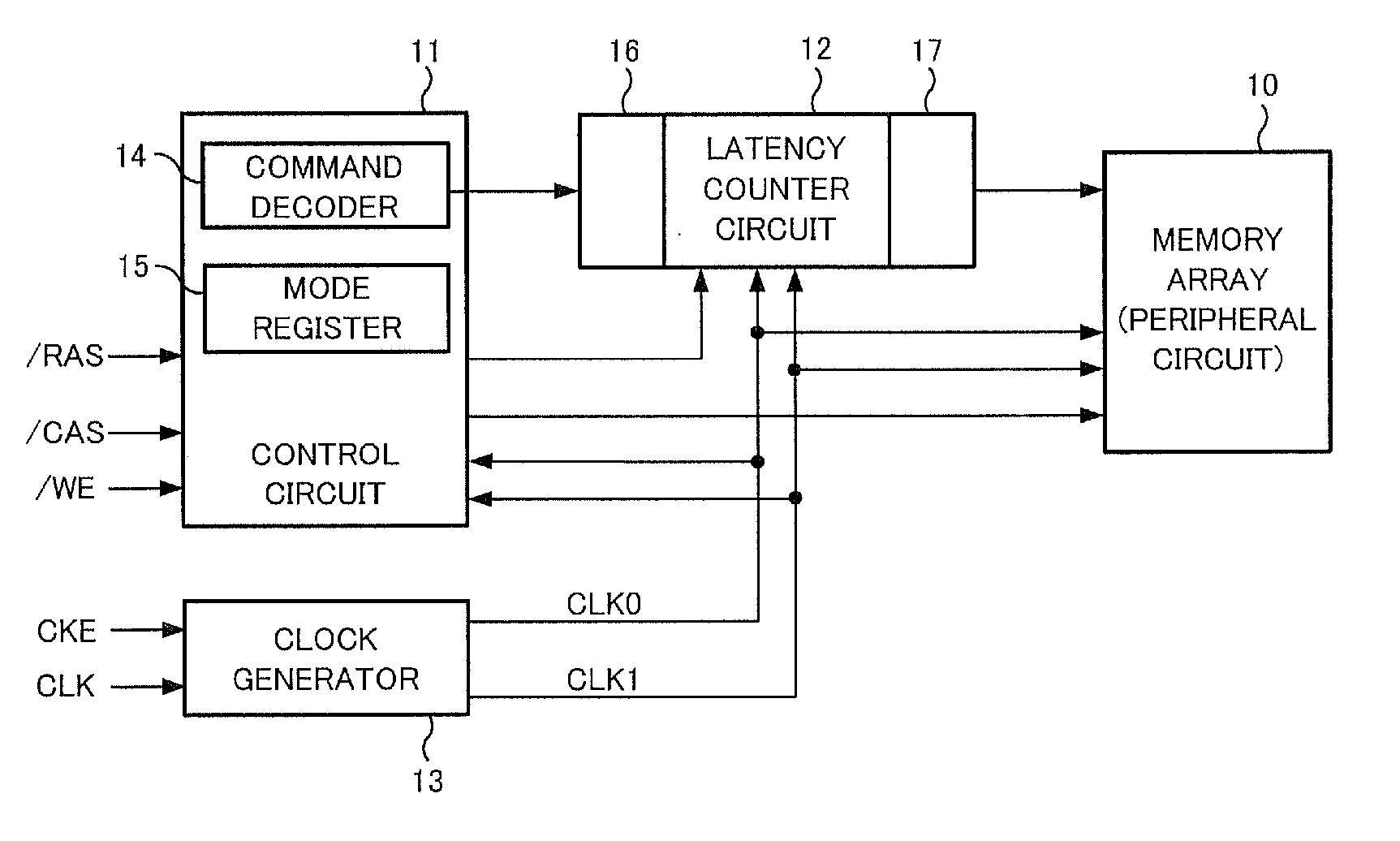
[0031]FIG. 1 is a block diagram showing a principal configuration of a synchronous semiconductor memory device of a first embodiment. The synchronous semiconductor memory device as shown in FIG. 1 includes a memory array 10, a control circuit 11, a latency counter circuit 12 and a clock generator 13. Further, there are provided a command decoder 14 and a mode register 15 which are included in the control circuit 11, and there are also provided an input command latch circuit 16 and an output command latch circuit 17 which are attached to the latency counter circuit 12. Actually the synchronous semiconductor memory device includes many other components, but only components related to the function based on the present invention are shown in FIG. 1.

[0032]In the above-mentioned configuration, the memory array 10 includes a plurality of memory cells formed at intersections of a plurality of word lines and a plurality of bit lines arranged in a matrix, and a read / write operation is perform...

second embodiment

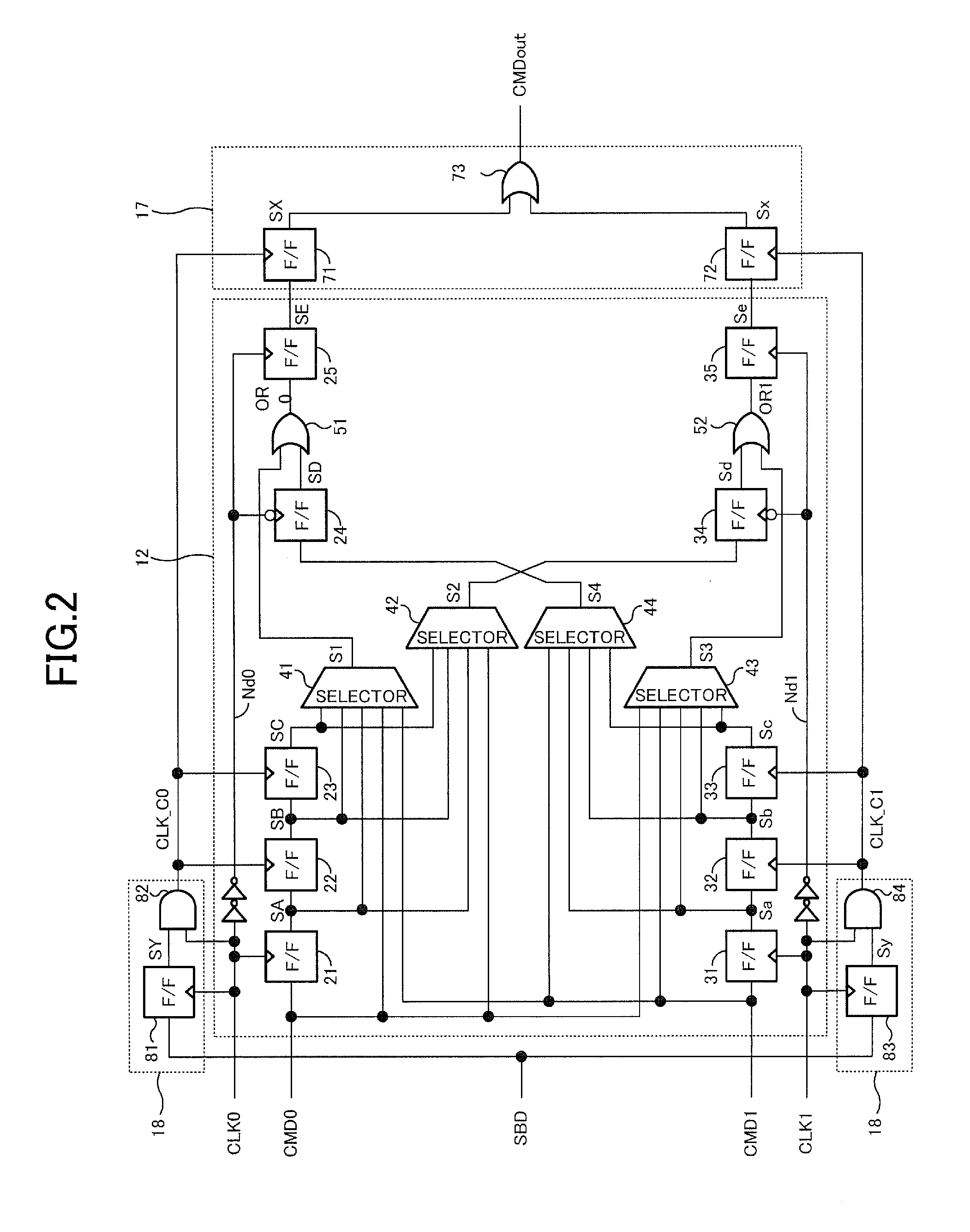
[0064]Next, a synchronous semiconductor memory device of a second embodiment will be described. A principal configuration of the synchronous semiconductor memory device of the second embodiment is common to the block diagram of FIG. 1, so description thereof is omitted. In the second embodiment, configurations of the latency counter circuit 12 and the clock control circuits 18 in FIG. 2 are changed, and they will be represented as a latency counter circuit 12a and clock control circuits 18a below.

[0065]FIG. 8 shows a configuration example of an area including the latency counter circuit 12a, the output command latch circuit 17 and the clock control circuits 18a. The latency counter circuit 12a shown in FIG. 8 can count nine steps of latencies 3 to 11 arbitrarily within the range from the minimum latency 3 to the maximum latency 11, in the same manner as the first embodiment. Here, the input command latch circuit 16 of the second embodiment has the same configuration as in FIG. 3 of ...


PUM


Abstract

A semiconductor device includes a latency setting circuit setting the latency, an input command circuit outputting a normal-phase (reverse-phase) command signal obtained by capturing an input command signal using a normal-phase (reverse-phase) clock, first and second counter circuits each including latch circuits for sequentially shifting the normal-phase (reverse-phase) command signal based on the normal-phase (reverse-phase) clock, a selector circuit controlling a signal path so that the normal-phase (reverse-phase) command signal is transmitted through the first (second) counter circuit when an even latency is set and the normal-phase (reverse-phase) command signal is transmitted so as to be shifted from the first (second) counter circuit to the second (first) counter circuit when an odd latency is set, and a control circuit controlling so that the latch circuits of the first (second) counter circuit are activated in response to the input command signal and stopped after an operation period is elapsed.

Description

BACKGROUND OF THE INVENTION[0001]1. Field of the Invention[0002]The present invention relates to a semiconductor device which operates in synchronization with a clock, and particularly relates to a synchronous semiconductor device having a configuration for controlling operation timings after issuing various commands in response to latencies.[0003]2. Description of Related Art[0004]Recently SDRAM (Synchronous Dynamic Random Access Memory) of DDR (Double Data Rate) type has been a mainstream as a synchronous semiconductor memory device to allow high speed operation. Since this DDR-SDRAM (referred to as DDR-SDRAM hereinafter) is provided with a latency counter in which the number of clock cycles required between issuing a command and completing data transmission in read / write operation is set as a latency and the set latency is counted based on an internal clock. In the DDR-SDRM, different latencies are defined for various types of operations and a user can preset a desired latency in...

Claims


Application Information

Patent Timeline
Patent Type & Authority Applications(United States)
IPC IPC(8): G11C8/00G11C8/18
CPCG11C7/1066G11C7/1072G11C2207/2272G11C7/222G11C11/4076G11C7/22
Inventor KINOSHITA, HIROTOFUJISAWA, HIROKI
Owner LONGITUDE SEMICON S A R L
Why Eureka
Try Eureka