Threshold Adjustment for High-K Gate Dielectric CMOS

a gate dielectric and threshold voltage technology, applied in the field of electronic devices, can solve the problems of affecting the achievement of the desired threshold voltage value, affecting the performance improvement of devices of deeply sub-micron generation, and increasing complexity of technology

Inactive Publication Date: 2009-11-26
GLOBALFOUNDRIES INC
View PDF13 Cites 16 Cited by
  • Summary
  • Abstract
  • Description
  • Claims
  • Application Information

AI Technical Summary

Benefits of technology

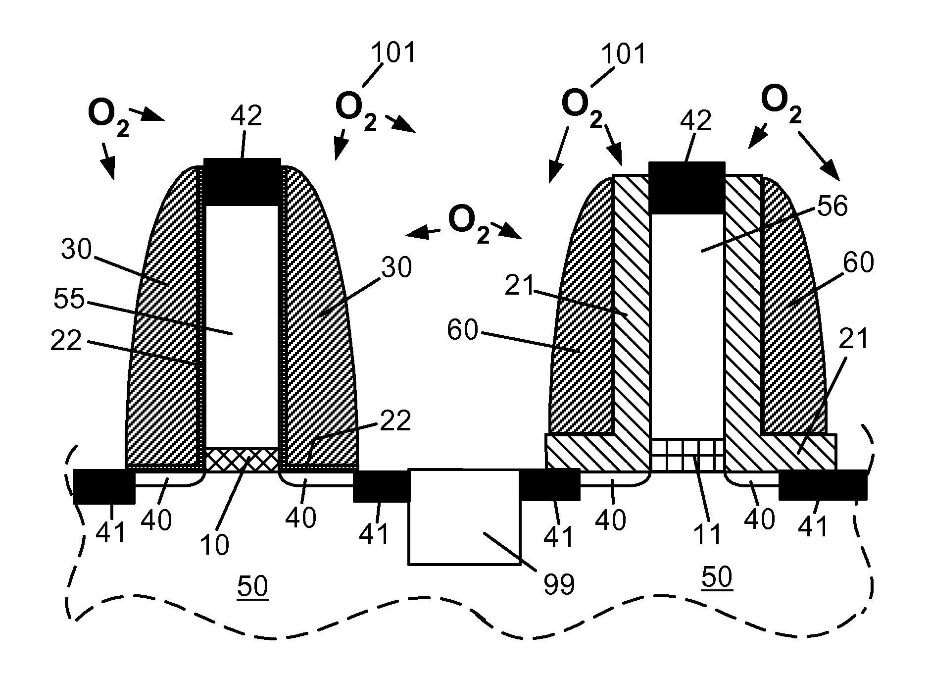
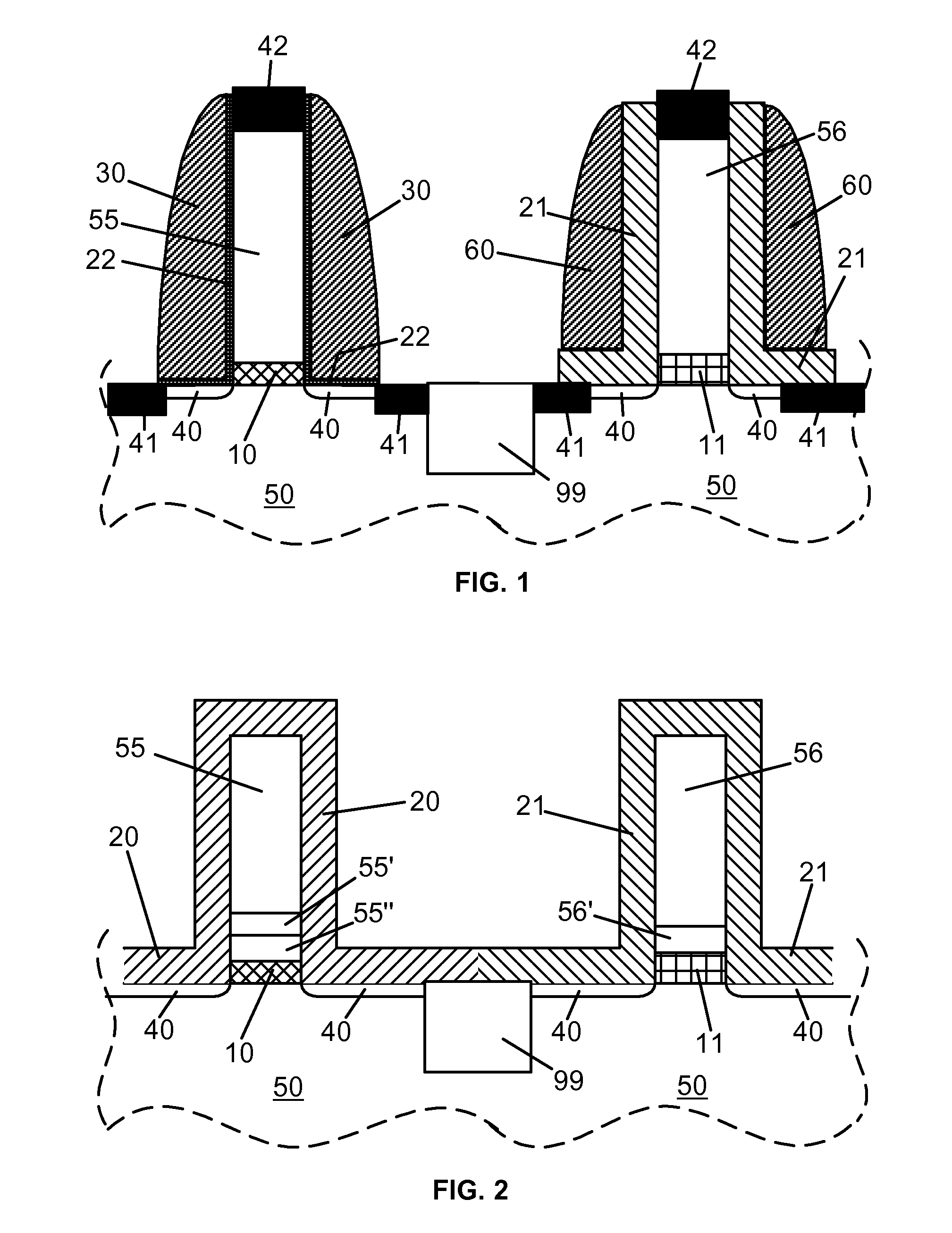
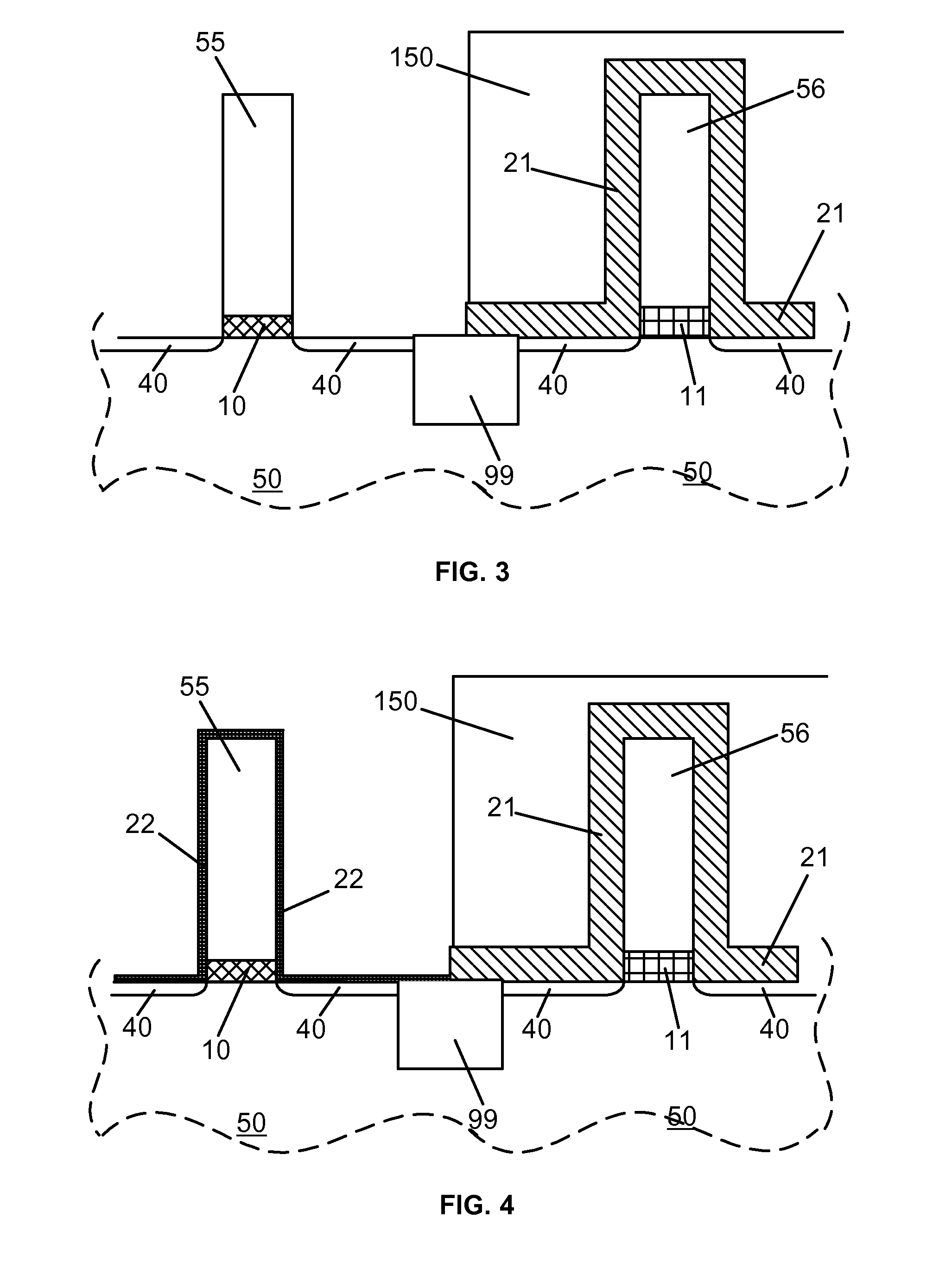
[0007]In view of the discussed difficulties, embodiments of the present invention discloses a CMOS structure, which contains at least one first type FET device and at least one second type FET device. The first type FET contains a first gate insulator which has a first high-k dielectric. The first type FET also has a first liner composed of oxide and having thickness between about 0.2 nm and 1.2 nm. The second type FET contains a second gate insulator which has a second high-k dielectric. The second type FET also has a second liner composed of oxide and with a thickness at least three times larger than the thickness of the first liner. As a result, when the structure is exposed to oxygen, oxygen is capable to reach the second high-k dielectric through the second liner, and shift the threshold voltage of the second type of FET, without affecting the threshold of the first type FET.

Problems solved by technology

As FET (Field-Effect-Transistor) devices are being scaled down, the technology becomes more complex, and changes in device structures and new fabrication methods are needed to maintain the expected performance enhancement from one generation of devices to the next.
There is a great difficulty in maintaining performance improvements in devices of deeply sub micron generations.
Sometimes such influences are detrimental for achieving the desired threshold voltage values.
Unfortunately, shifting the threshold of both PFET and NFET devices simultaneously, may not easily lead to threshold values in an acceptable tight range for CMOS circuits.

Method used


Image

  • Threshold Adjustment for High-K Gate Dielectric CMOS
  • Threshold Adjustment for High-K Gate Dielectric CMOS
  • Threshold Adjustment for High-K Gate Dielectric CMOS

Examples


Embodiment Construction

[0016]It is understood that Field Effect Transistor-s (FET) are well known in the electronic arts. Standard components of a FET are the source, the drain, the body in-between the source and the drain, and the gate. The gate is overlaying the body and is capable to induce a conducting channel in the body between the source and the drain. In the usual nomenclature, the channel is hosted by the body. The gate is typically separated from the body by the gate insulator. There are two type of FET devices: a hole conduction type, called PFET, and an electron conduction type, called NFET. Often PFET and NFET devices are wired into CMOS circuits. A CMOS circuit contains at least one PFET and at least one NFET device. In manufacturing, or processing, when NFET and PFET devices are fabricated together on the same chip, one is dealing with CMOS processing and the fabrication of CMOS structures. In FET operation, an electrical attribute is the threshold voltage. When the voltage between the gate...


PUM


Abstract

A CMOS structure is disclosed in which a first type FET has an extremely thin oxide liner. This thin liner is capable of preventing oxygen from reaching the high-k dielectric gate insulator of the first type FET. A second type FET device of the CMOS structure has a thicker oxide liner. As a result, an oxygen exposure is capable to shift the threshold voltage of the second type of FET, without affecting the threshold value of the first type FET. The disclosure also teaches methods for producing the CMOS structure in which differing type of FET devices have differing thickness liners, and the threshold values of the differing type of FET devices is set independently from one another.

Description

CROSS REFERENCE TO A RELATED APPLICATION[0001]This application is a Division of application Ser. No. 11 / 743,101, filed May 1, 2007, which is incorporated herein by reference in its entirety.FIELD OF THE INVENTION[0002]The present invention relates to electronic devices. In particular, it relates to CMOS structures having high-k containing gate dielectrics, and to ways to adjust the threshold voltage for the two type of devices independently from one another.BACKGROUND OF THE INVENTION[0003]Today's integrated circuits include a vast number of devices. Smaller devices and shrinking ground rules are the key to enhance performance and to reduce cost. As FET (Field-Effect-Transistor) devices are being scaled down, the technology becomes more complex, and changes in device structures and new fabrication methods are needed to maintain the expected performance enhancement from one generation of devices to the next. The mainstay material of microelectronics is silicon (Si), or more broadly, ...

Claims


Application Information

Patent Timeline
Patent Type & Authority Applications(United States)
IPC IPC(8): H01L21/8238
CPCH01L21/28176H01L29/6656H01L27/092H01L21/823864Y10S438/981H01L21/8238
Inventor DORIS, BRUCE B.CARTIER, EDUARD ALBERTNARAYANAN, VIJAYPARUCHURI, VAMSI
Owner GLOBALFOUNDRIES INC
Why Eureka
Try Eureka