Plasma processing apparatus

a processing apparatus and plasma technology, applied in the direction of electrical apparatus, plasma technique, electric discharge tubes, etc., can solve the problems of long time-consuming and laborious etching, inability to satisfactorily etch by simply chipping, and generation of dust, so as to achieve high efficiency, simple structure, and low cost.

Inactive Publication Date: 2009-12-03
ULVAC INC
View PDF5 Cites 11 Cited by
  • Summary
  • Abstract
  • Description
  • Claims
  • Application Information

AI Technical Summary

Benefits of technology

[0052]With the system configured as the above, it is not necessary to provide a radio frequency power source for the opposite electrode separately. Therefore, the structure can be simplified, which makes the system inexpensive. Furthermore, it is possible to form highly effective plasma without involving any problem such that radio frequency fields to be applied interfere with each other. In addition, radio frequency having a predetermined voltage value can be applied to the opposite electrode through the floating electrode. Therefore, it is possible to improve resistance of a mask and achieve a satisfactory etching rate.
[0053]Additionally, there has been a problem, with respect to a ICP plasma source or ECR plasma source, in that materials generated by discomposing gas by means of plasma stick to the wall and the stuck materials fall down to the surface of the substrate as dust. However, an opposite electrode being in a floating state is provided above the substrate and radio frequency power is applied to the opposite electrode. By doing this, ions included in plasma conti...

Problems solved by technology

In the case of the magnetic neutral loop discharge etching apparatus shown in FIG. 1, there has been a problem in that, when the relevant system is employed to etch a resist pattern having a fine structure with use of halogen etching gas, the film deposited on the inner face of the top plate exfoliates by etching for a long time, thereby generating dust.
However, the etching cannot be carried out satisfactorily by simply chipping.
On the contrary, in the case where the protective material is far too little than the etchant, the wall is eroded by the etchant.
As a result, bowing occurs on the wall so that the desirable shape cannot be obtained.
However, if the easily polymerizing material reaches the wall of a discharge chamber, the relevant material adheres to the wall and causes dust.
If the pore is of very small size, electrons do not sufficiently flow into the pore due to a sheath electric field.
Therefore, a charge in the pore cannot be corrected and positive charge-up occurs.
As a result, positive ions are prevented from flowing into the pore and thus etching cannot progress satisfactorily.
Meanwhile, in regard to an ICP plasma source and an ECR plasma source, a problem lies in that a material generated by decomposing gas by means of plasma adheres to the wall and the adhered material exfoliates before long and falls down on the surface of the substrate as dust.
Fur...

Method used


Image

  • Plasma processing apparatus
  • Plasma processing apparatus
  • Plasma processing apparatus

Examples


Embodiment Construction

[0061]Hereinafter, embodiments of the present invention will be described with reference to FIGS. 3 to 6 of the accompanying drawings.

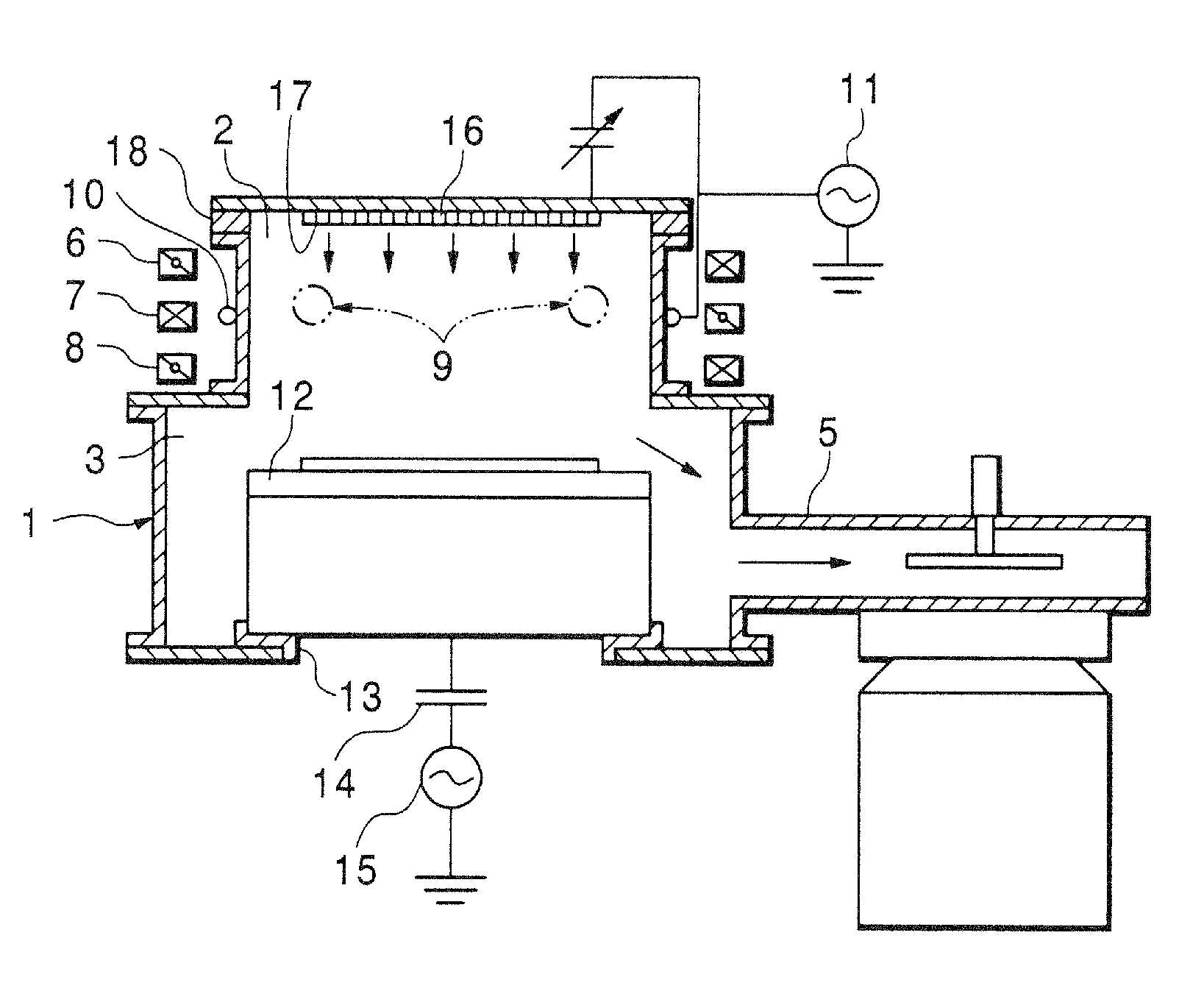
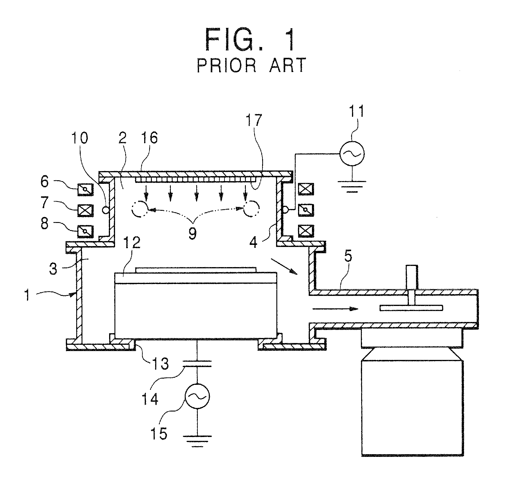
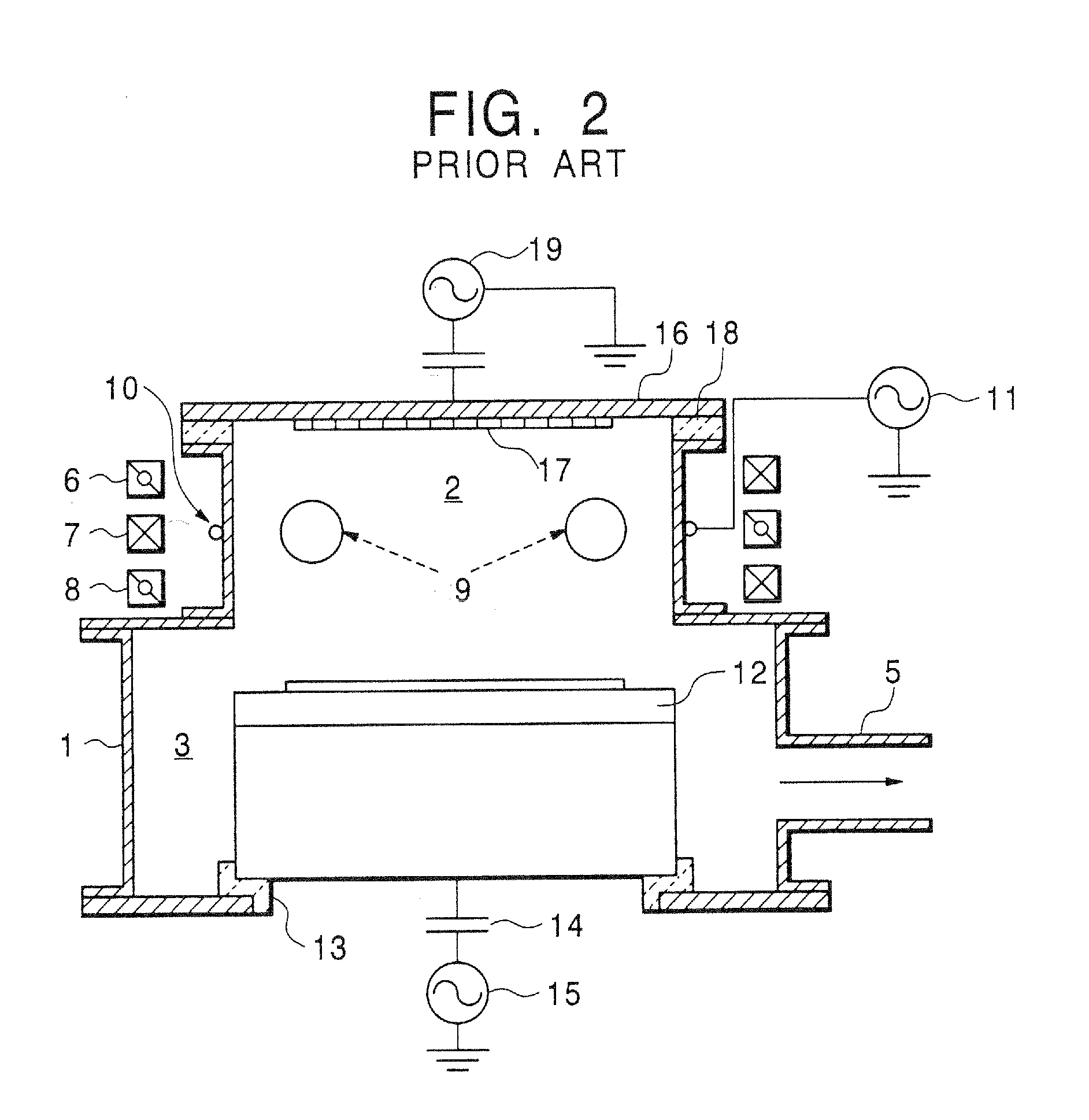
[0062]FIG. 3 shows a schematic structure of a magnetic neutral loop discharge etching apparatus of the invention. In FIG. 3, the same constituting elements as those of the conventional example shown in FIGS. 1 and 2 are indicated by the same reference numerals and the detailed descriptions for those elements will be omitted.

[0063]The etching apparatus shown in FIG. 3 employs a two frequency discharge method that is a modification of the aforementioned three-frequency discharge method. In this etching apparatus, a ground electrode provided at the position opposite to the substrate mounting electrode 12 is an opposite electrode whose potential is in a floating state by a dielectric so as to apply weak radio frequency bias power to the opposite electrode (top plate 16). Further, in this etching apparatus, a shunt is provided at an arbitrary position of a...


PUM

PropertyMeasurementUnit
Electric potential / voltageaaaaaaaaaa
Electric fieldaaaaaaaaaa

Abstract

The present invention is to provide a plasma processing apparatus, whose structure can be simplified, and further, which is capable of forming highly effective plasma and obtaining a satisfactory vertical etching property without involving a problem concerning interference. In the plasma processing apparatus according to the invention, a ground electrode provided at a position opposite to a substrate mounting electrode is configured to be a counter electrode, whose potential is in a floating state, and radio frequency power is branched at an arbitrary position of the radio frequency antenna coil, which generates inductive discharge, into the counter electrode through a capacitor so as to share a part of the radio frequency power used for inductive discharge, thereby generating a self-bias in the counter electrode. In the system, there is provided a mechanism for controlling the radio frequency voltage to be applied to the floating electrode uniformly.

Description

CROSS REFERENCE TO RELATED APPLICATIONS[0001]This is a Divisional of U.S. patent application Ser. No. 10 / 146,366 filed May 15, 2002, which claimed the priority of Japanese Patent Application 2001-149825 filed May 18, 2001 and 2001-305101 filed Oct. 1, 2001, the priority of all three applications are claimed and all three are incorporated herein by reference.BACKGROUND OF THE INVENTION[0002]1. Field of the Invention[0003]The present invention relates to a plasma processing apparatus, in particular, an etching apparatus that etches a thin film formed on a semiconductor substrate such as silicon or the like, materials for electronic devices, various glass, or various dielectrics, etc. with use of plasma.[0004]2. Prior Art[0005]In an etching apparatus in which gas is introduced into a vacuum chamber so as to form inductively coupled discharge plasma by radio frequency and a radio frequency power is applied to an electrode on which a substrate is mounted so as to generate a negative self...

Claims


Application Information

Patent Timeline
IPC IPC(8): C23F1/08H05H1/46H01J37/32H01L21/3065
CPCH01J37/321H01L21/3065
Inventor HAYASHI, TOSHIOCHEN, WEISUGITA, KIPPEIKAGA, KOUJI
Owner ULVAC INC
Why Eureka
Try Eureka