Organic light-emitting laminate and organic electroluminescent device conatiaing the same
- Summary
- Abstract
- Description
- Claims
- Application Information
AI Technical Summary
Benefits of technology
Problems solved by technology
Method used
Image

Examples
example 1
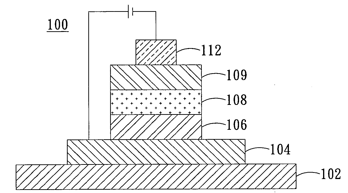
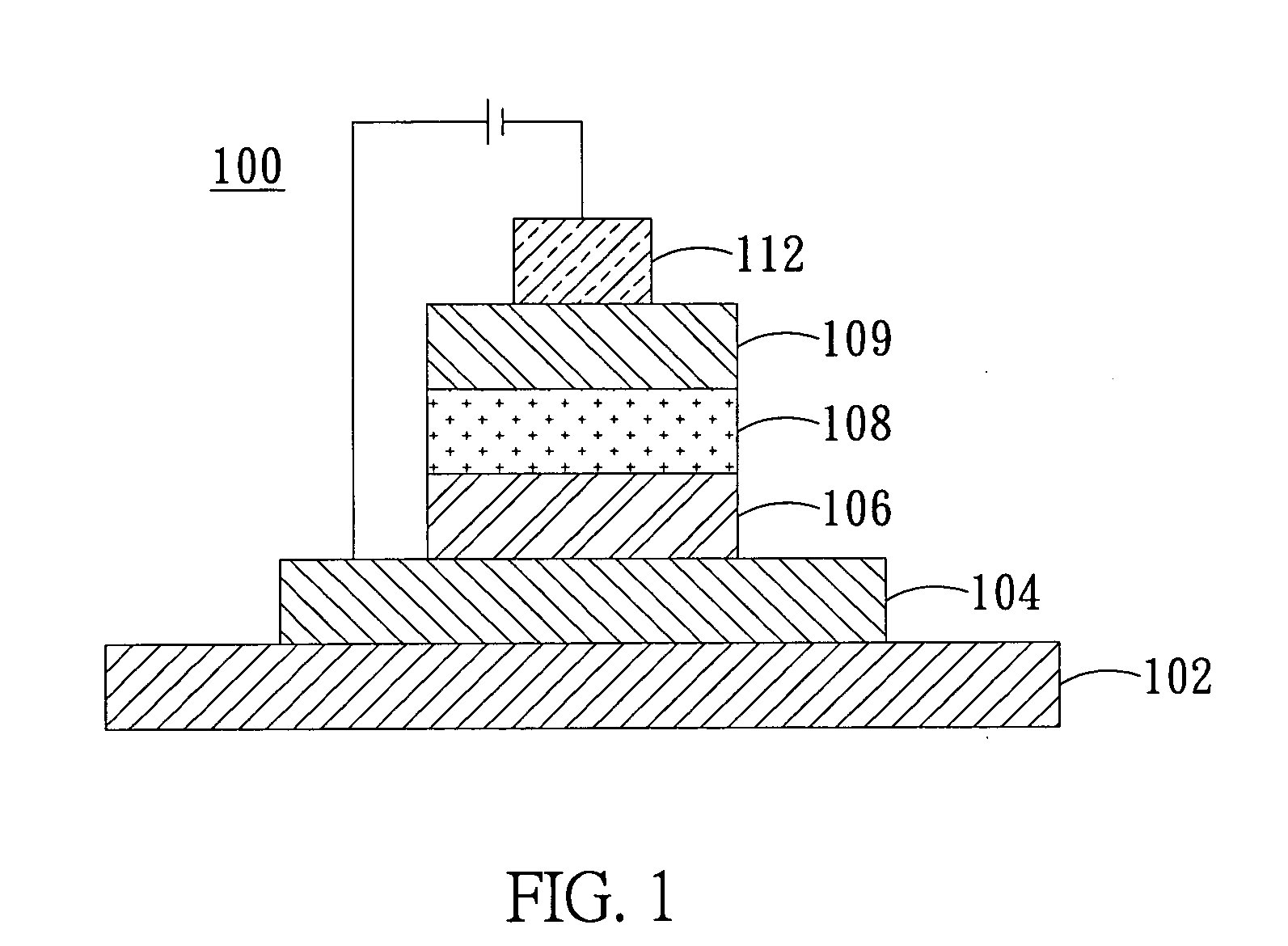
[0054]In the organic light-emitting laminate layer of this Example, CzSi was used as first and second main light-emitting materials; PO-01 and FIrpic were respectively used as first and second phosphorescent materials; and TCTA was used as carrier-transporting material.
[0055]A 150 nm thick layer of ITO (indium tin oxide) as anode layer was formed on a 0.7 nm thick glass substrate, then a 45nm thick layer of NPB as hole-transporting layer was deposited on the anode layer and a 15 nm thick layer of DTASi as electron-blocking layer was deposited on the hole-transporting layer, both deposited by thermal vaporization. Next, CzSi as first main light-emitting material and PO-01 as first phosphorescent material, in a weight ratio of 92:8, were co-deposited by vaporization on the electron-blocking layer to form a first light-emitting layer with a thickness of 10 nm, which emits yellow light. Next, CzSi as second main light-emitting material, FIrpic as second phosphorescent material and TCTA ...
example 2
[0056]In the organic light-emitting laminate layer of this Example, CzSi was used as first and second main light-emitting materials; PO-01 and FIrpic were respectively used as first and second phosphorescent materials; and DTASi was used as carrier-transporting material.
[0057]A 150 nm thick layer of ITO (indium tin oxide) as anode layer was formed on a 0.7 nm thick glass substrate, then a 45 nm thick layer of NPB as hole-transporting layer was formed on the anode layer and a 15 nm thick layer of DTASi as electron-blocking layer was formed on the hole-transporting layer, both deposited by thermal vaporization. Next, CzSi as first main light-emitting material and PO-01 as first phosphorescent material, in a weight ratio of 92:8, were co-deposited by vaporization on the electron-blocking layer to form a first light-emitting layer with a thickness of 10 nm, which emits yellow light. Next, CzSi as second main light-emitting material, FIrpic as second phosphorescent material and DTASi as ...
example 3
[0059]In the organic light-emitting laminate layer of this Example, 4CzPBP was used as first and second main light-emitting materials; PO-01 and FIrpic were respectively used as first and second phosphorescent materials; and TCTA was used as carrier-transporting material.
[0060]A 150 nm thick layer of ITO (indium tin oxide) as anode layer was formed on a 0.7 nm thick glass substrate, then a 45 nm thick layer of NPB as hole-transporting layer was formed on the anode layer and a 15 nm thick layer of DTASi as electron-blocking layer was formed on the hole-transporting layer, both deposited by thermal vaporization. Next, 4CzPBP as first main light-emitting material and PO-01 as first phosphorescent material, in a weight ratio of 85:15, were co-deposited by vaporization on the electron-blocking layer to form a first light-emitting layer with a thickness of 12 nm, which emits yellow light. Next, 4CzPBP as second main light-emitting material, FIrpic as second phosphorescent material and TCT...
PUM
 Abstract
Description
Claims
Application Information
 - R&D
- Intellectual Property
- Life Sciences
- Materials
- Tech Scout
- Unparalleled Data Quality
- Higher Quality Content
- 60% Fewer Hallucinations
Browse by: Latest US Patents, China's latest patents, Technical Efficacy Thesaurus, Application Domain, Technology Topic, Popular Technical Reports.
© 2025 PatSnap. All rights reserved.Legal|Privacy policy|Modern Slavery Act Transparency Statement|Sitemap|About US| Contact US: help@patsnap.com