

Surface-emitting laser array, optical scanning device, and image forming device
a laser array and surface-emitting technology, applied in semiconductor lasers, instruments, recording devices, etc., can solve the problems of difficult to carry out uniform mesa etching on the surface of the wafer, difficult to control the depth of etching, and difficult to carry out mesa etching, so as to prevent the exposure prevent the oxidization of the first reflection layer
- Summary
- Abstract
- Description
- Claims
- Application Information
AI Technical Summary
Benefits of technology
Problems solved by technology
Method used
Image

Examples
Embodiment Construction
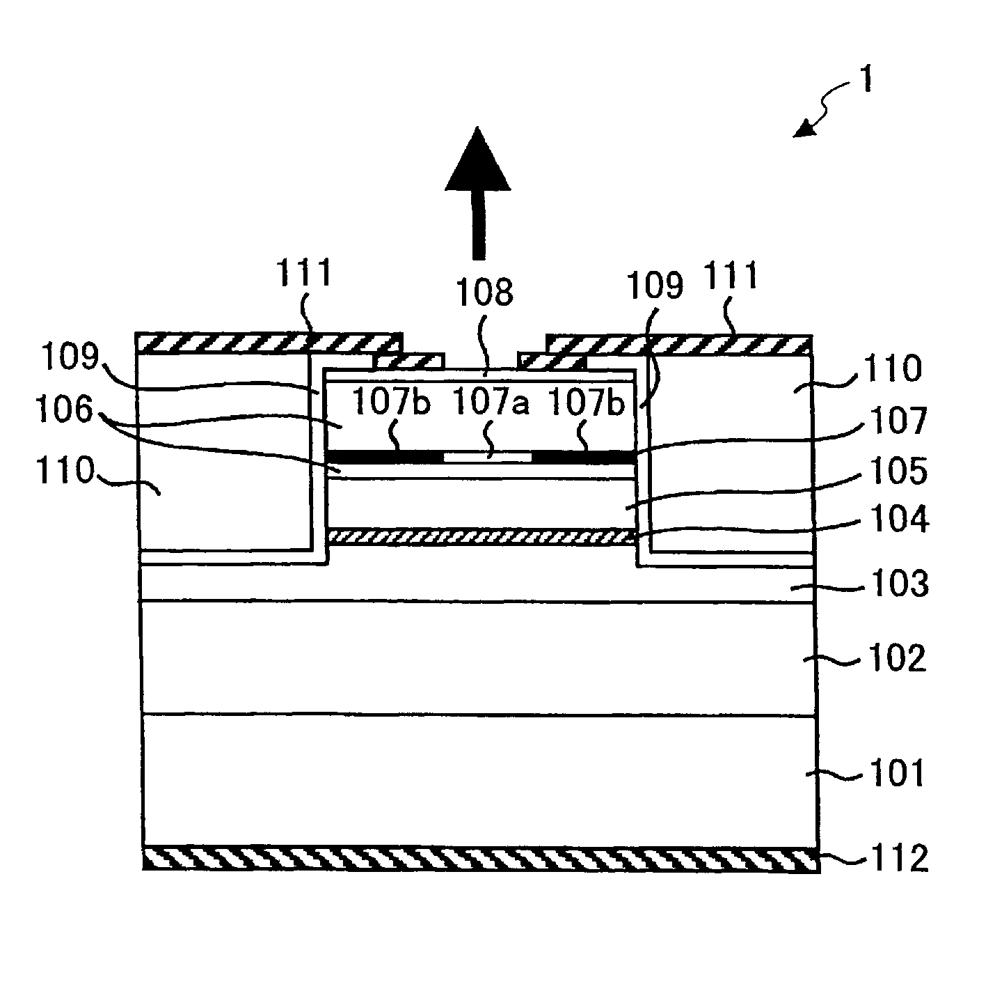
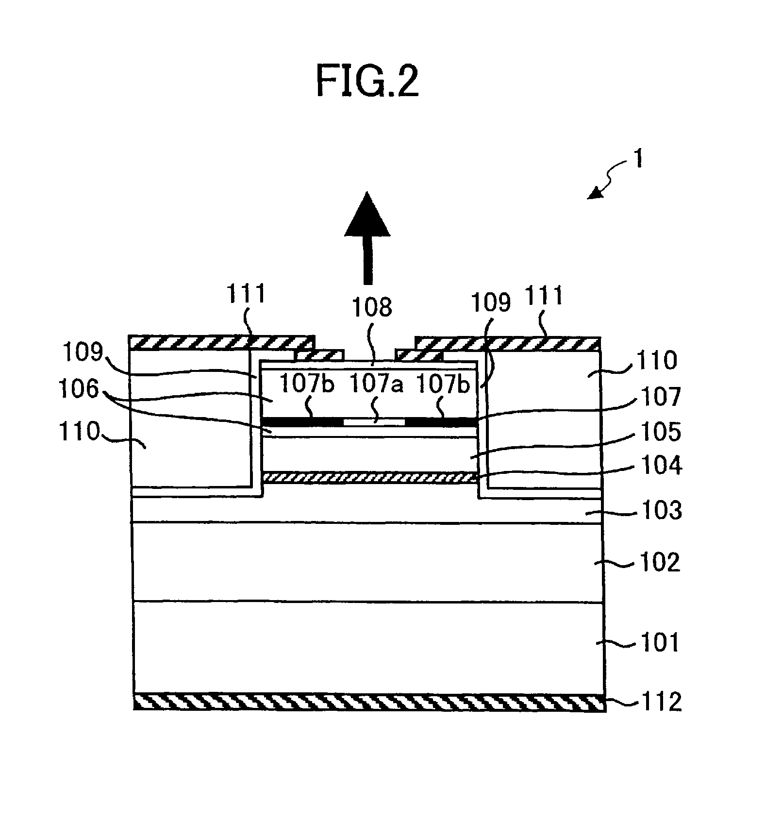
[0088]A description will be given of embodiments of the invention with reference to the accompanying drawings.
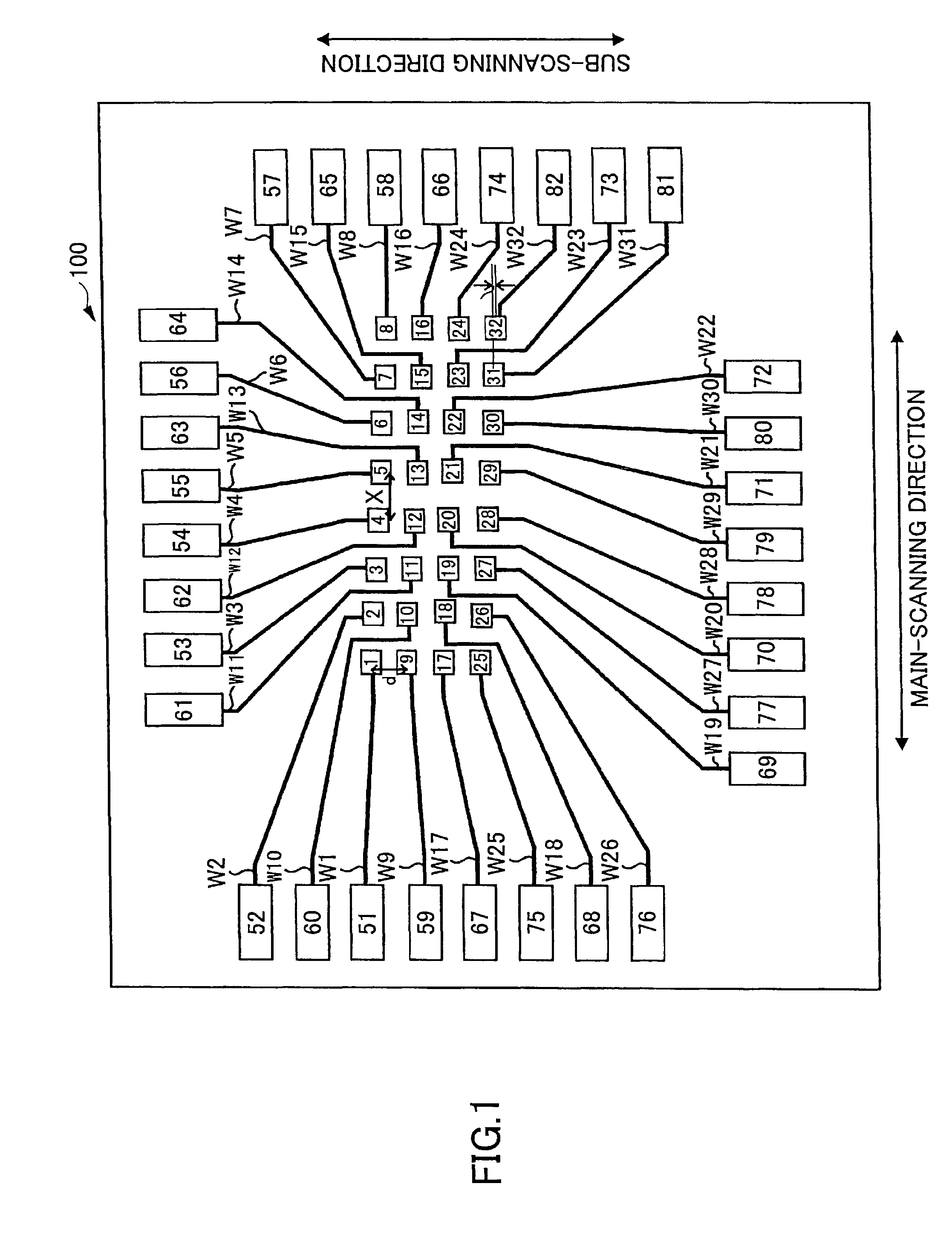
[0089]FIG. 1 is a plan view of a surface-emitting laser array in an embodiment of the invention. As shown in FIG. 1, the surface-emitting laser array 100 of this embodiment includes surface-emitting laser elements 1-32, pads 51-82, and wires W1-W32.
[0090]The surface-emitting laser elements 1-32 are arranged in the two-dimensional formation of four rows×eight columns. Each of the surface-emitting laser elements 1-32 has the rectangle form whose one side is 16 micrometers.
[0091]And the columns of four surface-emitting laser elements 1, 9, 17, 25 / 2, 10, 18, 26 / 3, 11, 19, 27 / 4, 12, 20, 28 / 5, 13, 21, 29 / 6, 14, 22, 30 / 7, 15, 23, 31 / 8, 16, 24, 32 are arranged in the sub-scanning direction. And the rows of eight surface-emitting laser elements 1-8 / 9-16 / 17-24 / 25-32 are arranged in the main scanning direction.
[0092]The rows of the eight surface-emitting laser elements 1-8 / 9-16 / 17-24 / 2...
PUM
 Abstract
Description
Claims
Application Information