Dividing method for wafer having film on the front side thereof

a technology of dividing method and wafer, which is applied in the direction of manufacturing tools, laser beam welding apparatus, welding/soldering/cutting articles, etc., can solve the problem that the film formed on the surface of each street cannot be divided by this method

Active Publication Date: 2009-12-03
DISCO CORP
View PDF2 Cites 37 Cited by
  • Summary
  • Abstract
  • Description
  • Claims
  • Application Information

AI Technical Summary

Benefits of technology

[0007]It is therefore an object of the present invention to provide a wafer dividing method which can divide a wafer having a film on the front side thereof without leaving the film along the street.

Problems solved by technology

However, in the case that the surface of each street is covered with a film such as a metal film, fluorosilicate glass film, silicon oxide based passivation film (SiO2, SiON), polyimide (PI) based polymer film, fluorine based polymer film, and fluorinated amorphous carbon based compound film, the following problem arises.
However, the film formed on the surface of each street cannot be divided by this method.

Method used


Image

  • Dividing method for wafer having film on the front side thereof
  • Dividing method for wafer having film on the front side thereof
  • Dividing method for wafer having film on the front side thereof

Examples


Embodiment Construction

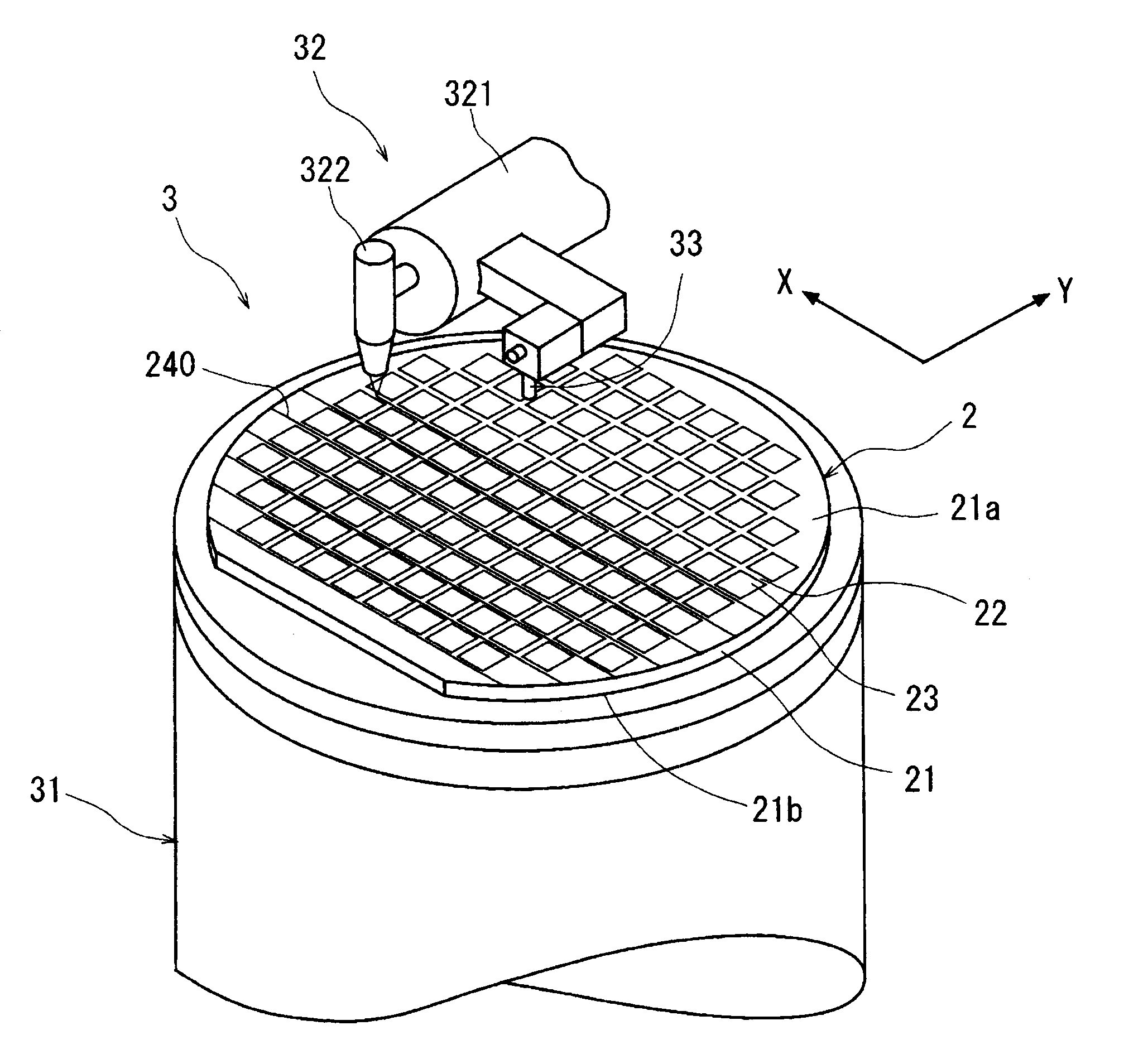
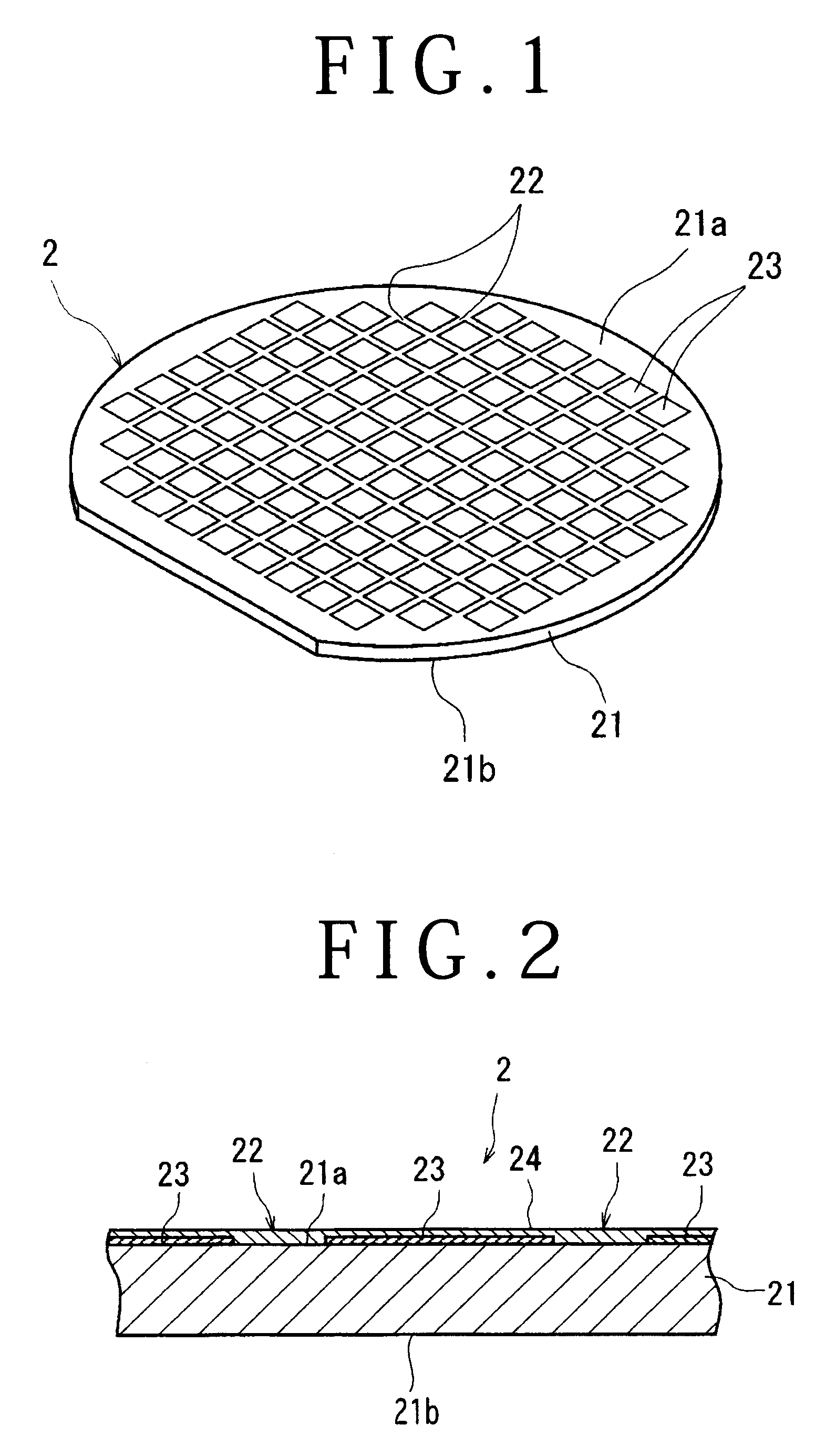
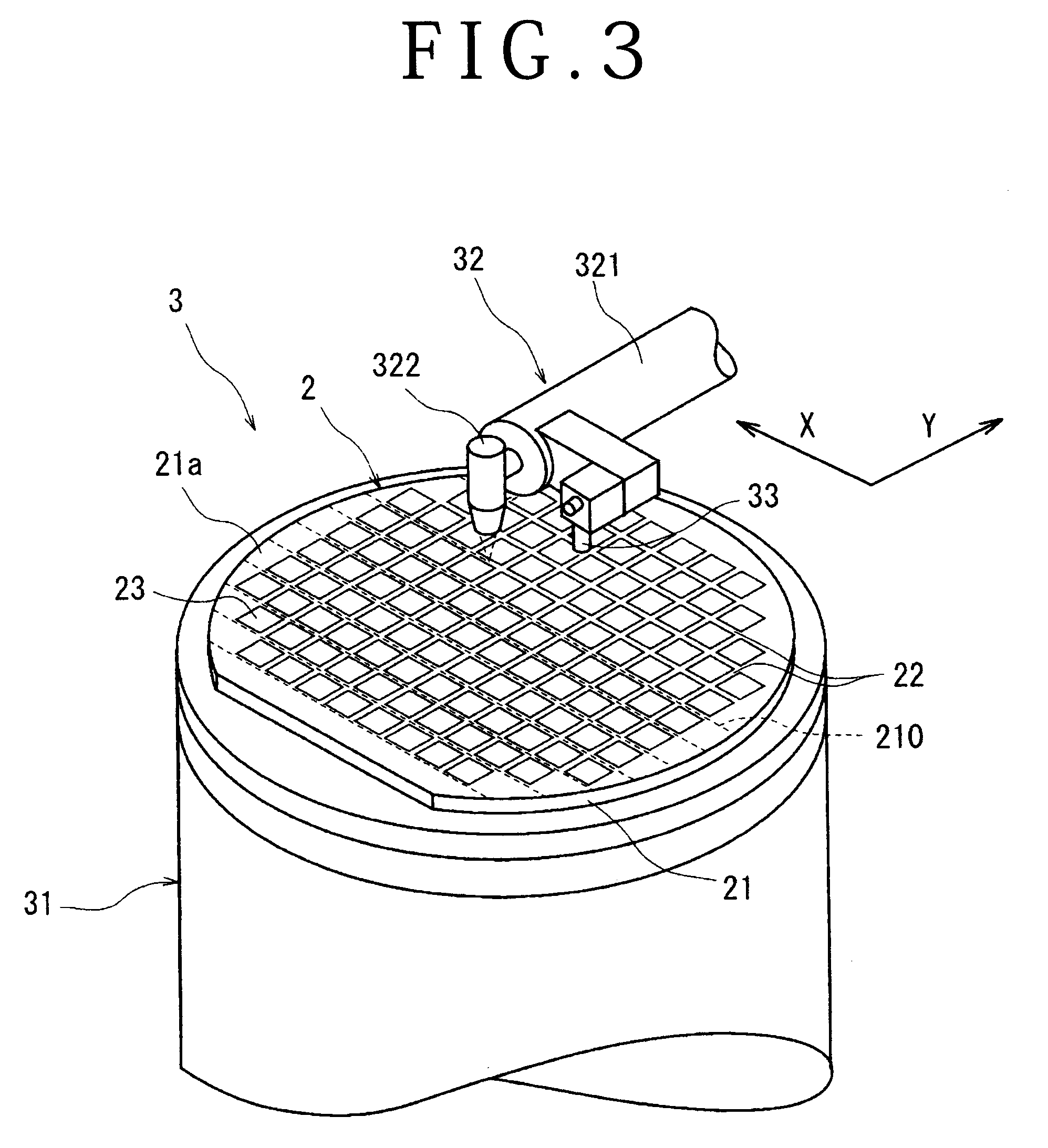
[0025]A preferred embodiment of the wafer dividing method according to the present invention will now be described in detail with reference to the attached drawings. FIG. 1 shows a perspective view of a wafer 2 to be divided by the wafer dividing method according to the present invention. FIG. 2 shows an enlarged sectional view of an essential part of the wafer 2 shown in FIG. 1. The wafer 2 shown in FIGS. 1 and 2 is formed from a silicon substrate 21 having a thickness of 600 μm, for example. A plurality of crossing streets 22 are formed on the front side 21a of the silicon substrate 21, thereby partitioning a plurality of rectangular areas in which a plurality of devices 23 such as ICs, LSIs, liquid crystal drivers, and flash memories are respectively formed. According to the embodiment as shown in FIG. 2, for the wafer 2, a polyimide (PI) based polymer film 24 is formed on the front side 21a of the silicon substrate 21 so as to fully cover the streets 22 and the devices 23.

[0026]...


PUM

PropertyMeasurementUnit
thicknessaaaaaaaaaa
transmission wavelengthaaaaaaaaaa
absorption wavelengthaaaaaaaaaa

Abstract

A wafer dividing method for dividing a wafer having a film on the front side thereof. The wafer dividing method includes a modified layer forming step of applying a laser beam having a transmission wavelength to the substrate of the wafer from the front side thereof along the streets so that a focal point of the laser beam is set inside the substrate, thereby forming a modified layer in the substrate along each street, a film dividing step of applying a laser beam having an absorption wavelength to the film from the front side of the wafer along each street to thereby form a laser processed groove for dividing the film along each street, a back grinding step of grinding the back side of the substrate of the wafer to thereby reduce the thickness of the wafer to a predetermined thickness, a wafer supporting step of attaching the wafer to a dicing tape supported to an annular frame, and a wafer breaking step of applying an external force to the wafer by expanding the dicing tape to thereby break the wafer along each street.

Description

BACKGROUND OF THE INVENTION[0001]1. Field of the Invention[0002]The present invention relates to a wafer dividing method for dividing a wafer into individual devices along a plurality of crossing streets formed on the front side of the wafer, wherein the devices are respectively formed in a plurality of areas partitioned by the streets.[0003]2. Description of the Related Art[0004]In a semiconductor device fabrication process, a plurality of crossing streets (division lines) are formed on the front side of a substantially disk-shaped semiconductor wafer to partition a plurality of areas where devices such as ICs, LSIs, liquid crystal drivers, and flash memories are respectively formed. The wafer is cut along the streets to divide these areas from each other along the streets, thereby producing the individual devices.[0005]As a method of dividing the wafer along the streets, a laser processing method using a pulsed laser beam having a transmission wavelength to the wafer has been prop...

Claims


Application Information

Patent Timeline
Patent Type & Authority Applications(United States)
IPC IPC(8): H01L21/304
CPCB23K26/0057B23K26/367H01L21/78B23K26/409B23K26/4075B23K26/40B23K26/364B23K26/53B23K2103/172B23K2103/50
Inventor WATANABE, YOSUKEOBA, RYUGONAKAMURA, MASARU
Owner DISCO CORP
Why Eureka
Try Eureka