High-isolation transmit/receive switch on CMOS for millimeter-wave applications

a millimeter-wave wireless transceiver and high-isolation technology, applied in transmission, multiple-port network, electrical equipment, etc., can solve the problems of reducing the breakdown voltage of the device, reducing the mobility constant of the carrier, and reducing the design difficulty of millimeter-wave wireless transceivers on the cmos chip, so as to save substantial space and eliminate one antenna

Active Publication Date: 2009-12-03
ADVANCED MICRO DEVICES INC +1
View PDF4 Cites 46 Cited by
  • Summary
  • Abstract
  • Description
  • Claims
  • Application Information

AI Technical Summary

Problems solved by technology

Unfortunately, compared to other much more expensive processes such as SiGe and GaAs, CMOS has greater process variability, lower carrier mobility constants, and smaller device breakdown voltages.
This makes the design of millimeter wave wireless transceivers on a CMOS chip particularly challenging.
Eliminating one antenna saves substantial space.
However, T / R switches must be a high performance component as transmitted signals are often magnitudes of order more powerful than received signals, meaning that even slight leakage of transmit signals to the receiver circuitry could saturate the receiver circuitry.
The lossy and relatively poor performance of CMOS makes T / R switch isolation very difficult to achieve, particularly at millimeter-wave frequencies.
However these technologies make costs much higher, make integration with other CMOS circuitry difficult, and do not permit system-on-a-chip in CMOS.
T / R switches might also be made using integrated bipolar junction transistor and CMOS (BiCMOS) technologies, or silicon on insulator (SOI) technology, however these also raise costs relative to CMOS processes.

Method used


Image

  • High-isolation transmit/receive switch on CMOS for millimeter-wave applications
  • High-isolation transmit/receive switch on CMOS for millimeter-wave applications
  • High-isolation transmit/receive switch on CMOS for millimeter-wave applications

Examples


Embodiment Construction

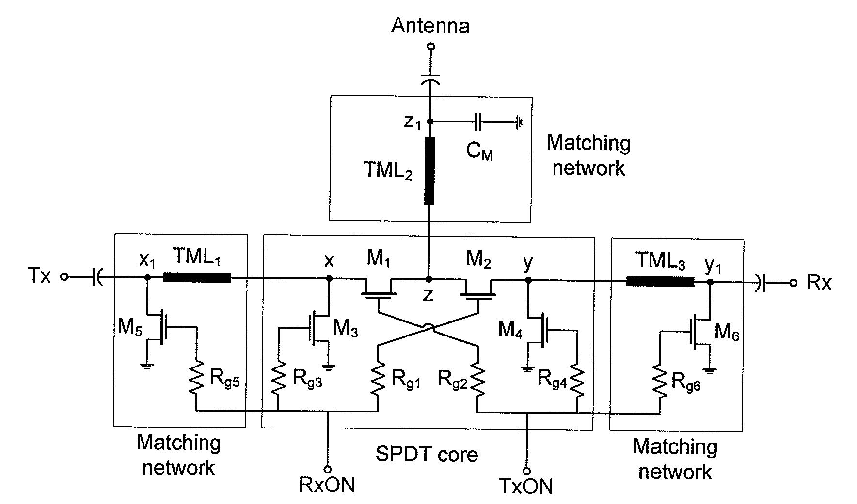
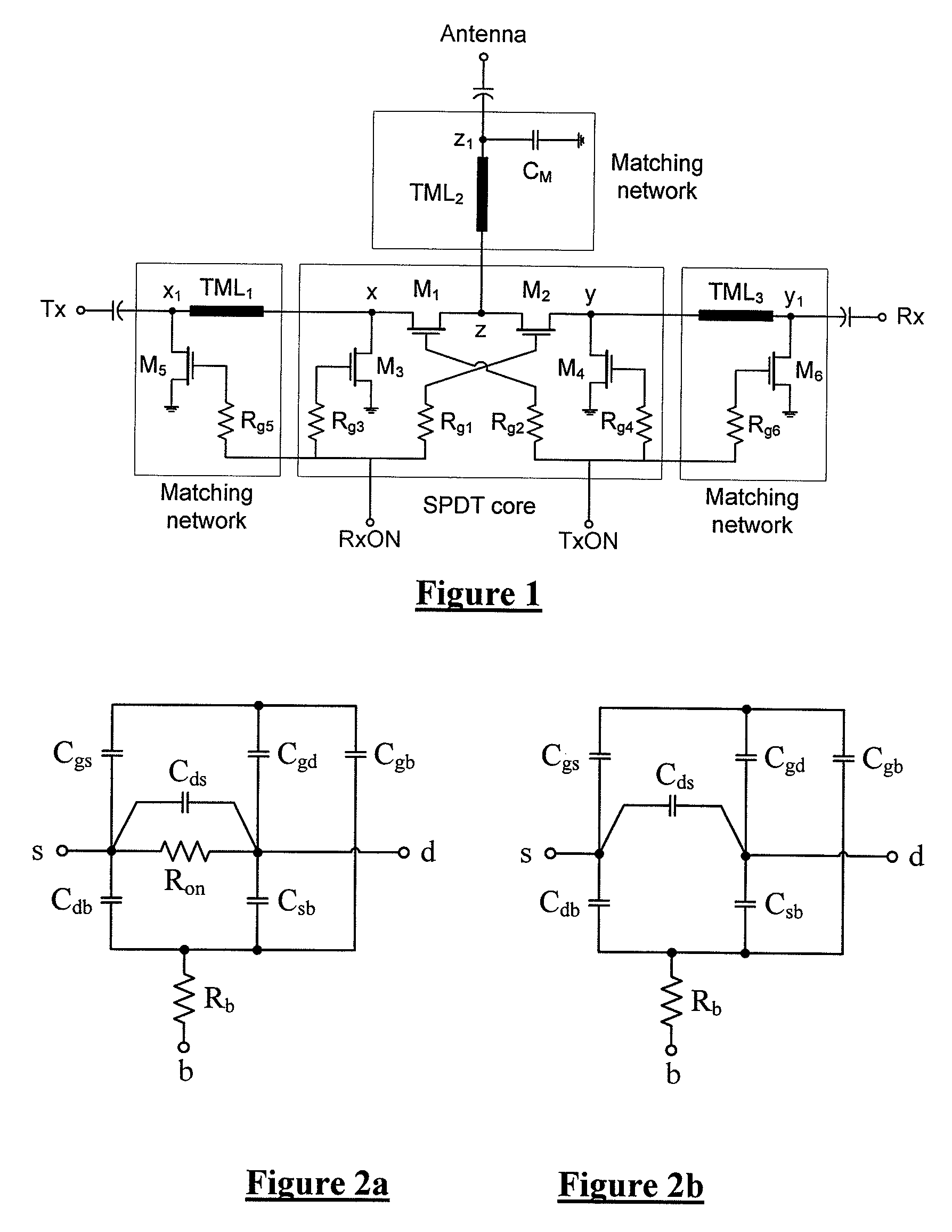
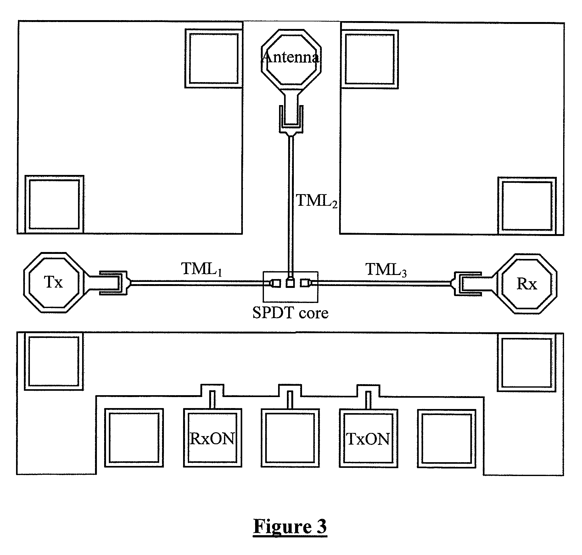
[0028]The 60-GHz band has been released for unlicensed use as a response to the demand of broadband wireless communications. The short wavelength at 60 GHz makes it possible to integrate the antennas and the RF transceiver on a single die. The present invention provides for a T / R switch to be employed so that a single antenna can be shared between the transmitter and the receiver to save area and cost of the chip. Even if an off-chip antenna is desired, an integrated T / R switch can still be used to reduce cost.

[0029]At millimeter-wave frequencies, the design of silicon-based T / R switches becomes much more challenging due to the coupling of the RF signals to the semiconductive silicon substrate. First, insertion loss is increased because of signal loss in the substrate. Second, isolation is decreased as a result of resistive coupling through the substrate. Apart from the detrimental effects of the silicon substrate, the low control voltage that accompanies deep submicron CMOS technol...


PUM


Abstract

A CMOS monolithic transmit / receive switch comprises a single pole double throw switch (SPDT) module operable to selectively connect an antenna port to either a transmit port or to a receive port. A transmit matching network comprising a first transmission line matches the impedance of the transmit port of the SPDT module to a transmit impedance, and a first shunt transistor is operable to selectively ground a transmitter end of the first transmission line. A receive matching network comprising a second transmission line matches the impedance of the receive port of the SPDT module to a receive impedance, and a second shunt transistor is operable to selectively ground a receiver end of the second transmission line.

Description

BACKGROUND OF THE INVENTION[0001]1. Field of the Invention[0002]The present invention relates to a transmit / receive switch which allows a millimeter wave antenna or antenna system to be shared for use by both a transmitter and by a receiver.[0003]2. Description of Related Art[0004]Modern wireless communications systems require transceivers that deliver gigabit speeds, are smaller in size, and have lower power consumption and cost. This motivates research to develop transceiver-on-chip and transceiver-in-a-package technologies. Recent advances in millimeter wave electronics have meant that significant portions of the system can now be integrated onto a single substrate or package. In order to achieve low costs and high digital integration, the complementary metal-oxide-semiconductor (CMOS) fabrication process is the process of choice as CMOS is the standard and a cost effective process for building digital circuits. Unfortunately, compared to other much more expensive processes such ...

Claims


Application Information

Patent Timeline
Patent Type & Authority Applications(United States)
IPC IPC(8): H04B1/44
CPCH04B1/48H01P1/15
Inventor TA, CHIEN M.SKAFIDAS, STANEVANS, ROB
Owner ADVANCED MICRO DEVICES INC
Why Eureka
Try Eureka