Optoelectronic display and method of manufacturing the same

a technology of optoelectronic display and manufacturing method, which is applied in the direction of discharge tube luminescnet display, electric discharge lamp, instruments, etc., can solve the problem of difficult to provide an intricately patterned colour-forming layer, and achieve the effect of negligible tooling costs

Active Publication Date: 2009-12-10
CAMBRIDGE DISPLAY TECH LTD
View PDF4 Cites 103 Cited by
  • Summary
  • Abstract
  • Description
  • Claims
  • Application Information

AI Technical Summary

Benefits of technology

[0033]Ink jet printing is particularly useful due to its scalability and adaptability. The former allows arbitrarily large sized substrates to be patterned and the latter...

Problems solved by technology

A problem with the aforementioned arrangements is that it is ...

Method used


Image

  • Optoelectronic display and method of manufacturing the same
  • Optoelectronic display and method of manufacturing the same
  • Optoelectronic display and method of manufacturing the same

Examples


Embodiment Construction

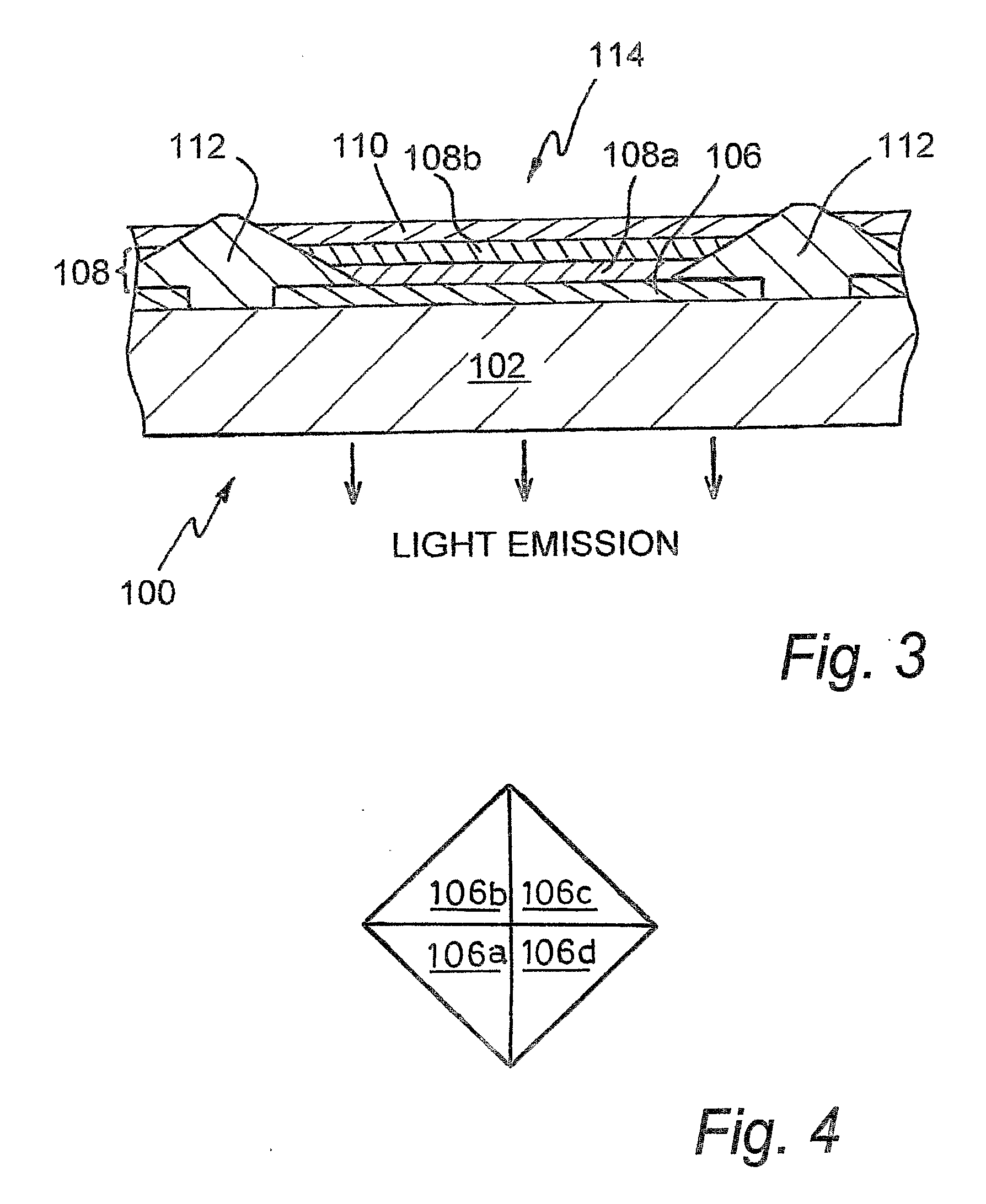
[0054]FIG. 3 shows a vertical cross section through an example of an OLED device 100. The structure of the device is somewhat simplified for the purposes of illustration.

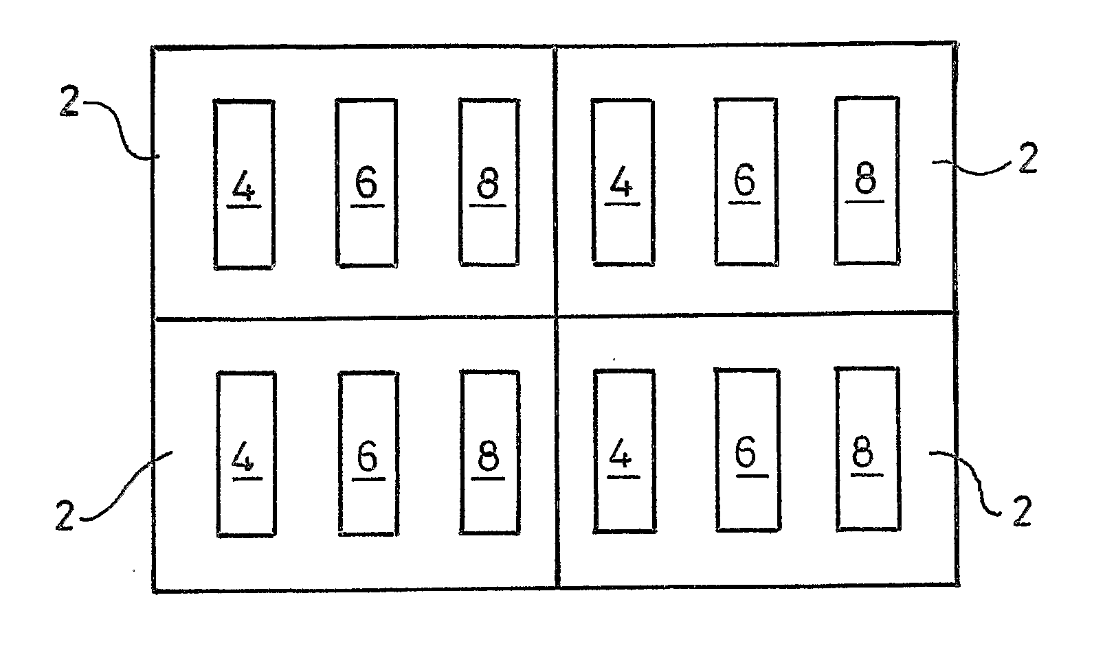
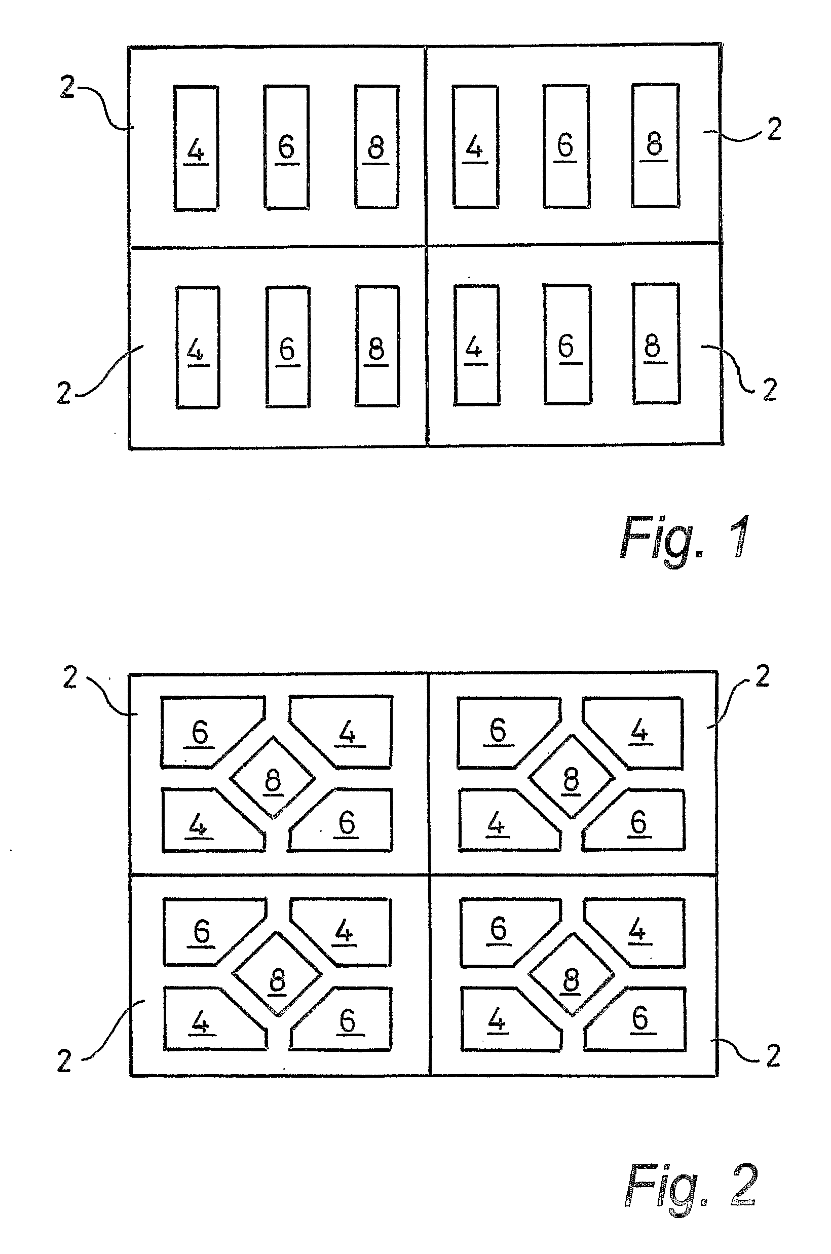
[0055]The OLED 100 comprises a substrate 102, typically 0.7 mm or 1.1 mm glass but optionally clear plastic, on which an anode layer 106 is deposited comprising four separately drivable sub-anodes (shown in FIG. 4). The anode layer typically comprises around 150 nm thickness of ITO (indium tin oxide), over which is provided a metal contact layer, typically around 500 nm of aluminium, sometimes referred to as anode metal. Glass substrates coated with ITO and contact metal may be purchased from Corning, USA. The contact metal (and optionally the ITO) is patterned as desired so that it does not obscure the display, by a conventional process of photolithography followed by etching.

[0056]A substantially transparent hole conducting layer 108a is provided over the anode metal, followed by an electroluminescent layer 108b. ...


PUM


Abstract

An optoelectronic display comprising a plurality of pixels, each pixel comprising a plurality of sub-pixels, wherein the optoelectronic display comprises a colour-forming layer which is patterned providing a plurality of discrete colour-forming regions in a two-dimensional array, and wherein an addressing array is provided for addressing the discrete colour-forming regions, at least some of the discrete colour-forming regions having portions which are separately addressable by the addressing array, each portion defining a sub-pixel of the optoelectronic display.

Description

FIELD OF INVENTION[0001]This invention relates to an optoelectronic display and a method of manufacturing the same.BACKGROUND OF INVENTION[0002]Various types of optoelectronic displays are known in the art. These include, for example, Liquid Crystal Displays (LCDs), ElectroLuminescent (EL) displays, and Plasma Displays (PDs).[0003]Multicoloured displays typically comprise a plurality of pixels, each pixel comprising a plurality of sub-pixels. In a full colour display, red, green, and blue sub-pixels are provided. The sub-pixels are defined by a colour-forming layer. The colour-forming layer may be a light-emissive layer comprising a plurality of discrete light-emissive regions of different light-emissive material defining the sub-pixels. For example, an EL display has such a light-emissive layer disposed between electrodes which are patterned so as to be able to address the individual sub-pixels which correspond to the discrete light-emissive regions of the light-emissive layer.[000...

Claims


Application Information

Patent Timeline
IPC IPC(8): H01L33/00H01L21/28
CPCH01L51/5203H01L27/3218H01L27/3216H01L27/3211G09G3/3208G09G2300/0452H10K59/352H10K59/353H10K50/805G09F9/302G09G3/3607H10K59/00
Inventor SMITH, EUANBALE, MARK
Owner CAMBRIDGE DISPLAY TECH LTD
Why Eureka
Try Eureka