Method for manufacturing semiconductor device

a manufacturing method and semiconductor technology, applied in semiconductor devices, semiconductor/solid-state device details, electrical apparatus, etc., can solve problems such as productivity decline, and achieve the effects of high reliability, reduced thickness and size, and easy production

Inactive Publication Date: 2009-12-10
SEMICON ENERGY LAB CO LTD
View PDF57 Cites 26 Cited by
  • Summary
  • Abstract
  • Description
  • Claims
  • Application Information

AI Technical Summary

Benefits of technology

[0033]Note that according to an embodiment of the present invention, a semiconductor device refers to a device which can function by utilizing the semiconductor characteristics. By using an embodiment of the present invention, a semiconductor device having a circuit including a semiconductor element (such as a transistor, a memory element, or a diode), and a semiconductor device such as a chip including a processor circuit can be manufactured.
[0034]With the use of the conductive shield covering a semiconductor integrated circuit, electrostatic breakdown (malfunctions of the circuit or damages of a semiconductor element) due to electrostatic discharge o

Problems solved by technology

In a semiconductor device (also referred to as a wireless signal processing unit, a semiconductor integrated circuit chip, or an IC chip) that sends and receives data by wireless communication through an antenna, breakdown (electrostatic breakdown) of the semiconductor device due to el

Method used


Image

  • Method for manufacturing semiconductor device
  • Method for manufacturing semiconductor device
  • Method for manufacturing semiconductor device

Examples


embodiment 1

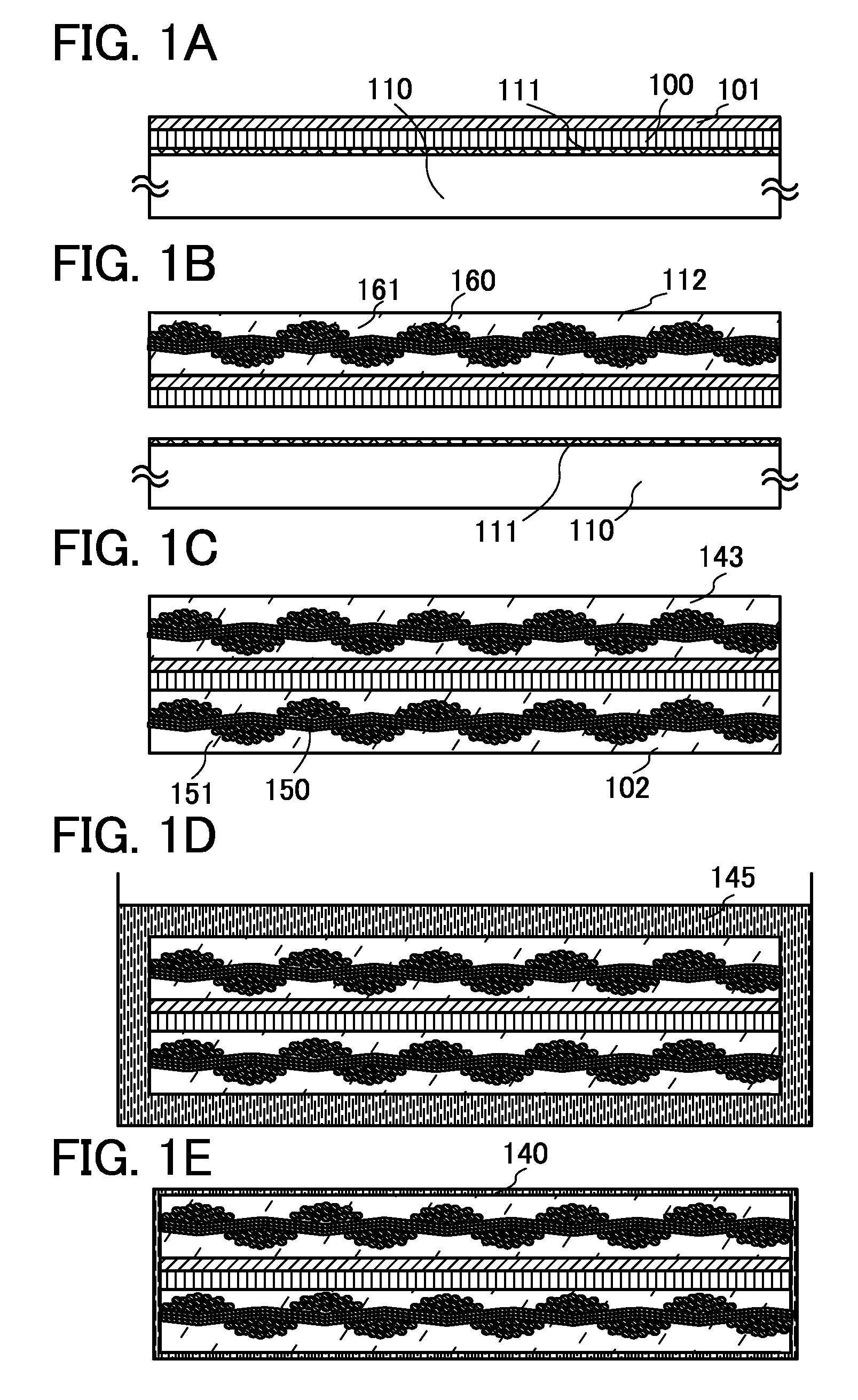
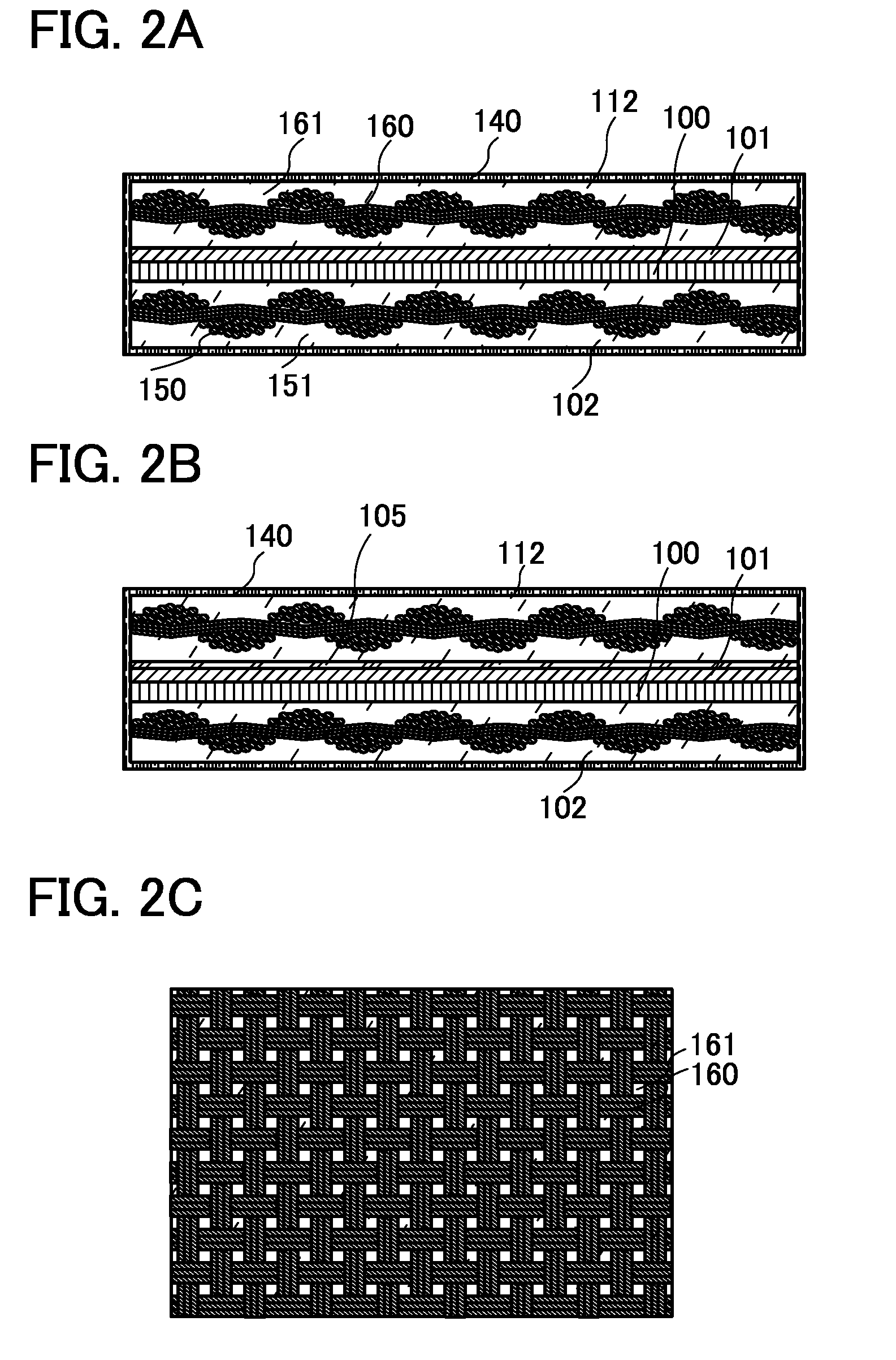
[0062]In this embodiment, a highly reliable semiconductor device and a method for manufacturing a semiconductor device with high yield will be described in detail with reference to FIGS. 1A to 1E, FIGS. 2A to 2C, and FIGS. 3A to 3C.

[0063]In a semiconductor device according to this embodiment, a semiconductor integrated circuit is separated from a substrate over which the semiconductor integrated circuit has been formed and is sandwiched between flexible insulators. Note that in this specification, the substrate over which the semiconductor integrated circuit has been formed is also referred to as a formation substrate. Thus, the semiconductor integrated circuit is formed over the formation substrate with a separation layer interposed therebetween.

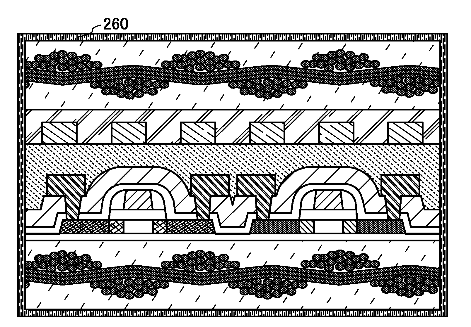
[0064]Semiconductor devices of this embodiment are illustrated in FIGS. 3A, 3B, and 3C. In FIG. 3A, an antenna 101 and a semiconductor integrated circuit 100 that is electrically connected to the antenna 101 are sandwiched between a first i...

embodiment 2

[0140]In this embodiment, another example of a semiconductor device for providing high reliability and a method for manufacturing the semiconductor device with the use of an embodiment of the present invention will be described with reference to FIGS. 14A and 14B, FIGS. 15A and 15B, FIGS. 16A to 16D, and FIGS. 17A to 17D. In the structure of this embodiment described below, a common reference numeral refers to the same part or a part having a similar function throughout drawings, in Embodiment 1 and this embodiment, and the description thereof is omitted.

[0141]An example in which an insulator has a stacked structure is described in this embodiment. In FIG. 14A, the antenna 101 and the semiconductor integrated circuit 100 that is connected to the antenna 101 are sandwiched between the first insulator 112 and the second insulator 102. A third insulator 103 is provided between the semiconductor integrated circuit 100 and the second insulator 102, and the conductive shield 140 is provid...

embodiment 3

[0167]In this embodiment, another example of a semiconductor device for providing high reliability and a method for manufacturing the semiconductor device with the use of an embodiment of the present invention will be described with reference to FIGS. 22A to 22C, FIGS. 23A1, 23A2, 23B1, and 23B2, and FIGS. 24A1 and 24A2. In the structure of this embodiment described below, a common reference numeral refers to the same part or a part having a similar function throughout drawings, in Embodiment 1 and Embodiment 2, and the description thereof is omitted.

[0168]In this embodiment, an example of a method for manufacturing a semiconductor device having an electrode layer that penetrates the inside of the semiconductor device as illustrated in FIGS. 22B and 22C in Embodiment 1 is described with reference to FIGS. 23A1, 23A2, 23B1, and 23B2, and FIGS. 24A1 and 24A2. FIGS. 23A2 and 23B2, and FIG. 24A2 are plan views, and FIGS. 23A1 and 23B1, and FIG. 24A1 are cross-sectional views taken along...


PUM


Abstract

An object is to provide a highly reliable semiconductor device that is reduced in thickness and size and has tolerance to external stress and electrostatic discharge. Another object is to prevent defective shapes and defective characteristics due to the external stress or an electrostatic discharge in the manufacturing process, and to manufacture a semiconductor device with high yield. Still another object is to manufacture a semiconductor device at low cost and with high productivity. With the use of a conductive shield covering a semiconductor integrated circuit, electrostatic breakdown (malfunctions of the circuit or damages of a semiconductor element) due to electrostatic discharge of the semiconductor integrated circuit is prevented. The conductive shield is formed so that at least the conductive shields on the top and bottom surfaces are electrically connected by a plating method. In addition, a semiconductor device can be formed at low cost with high productivity because a plating method is used for the formation of the conductive shield.

Description

BACKGROUND OF THE INVENTION[0001]1. Field of the Invention[0002]The present invention relates to a semiconductor device and a method for manufacturing the semiconductor device.[0003]2. Description of the Related Art[0004]In a semiconductor device (also referred to as a wireless signal processing unit, a semiconductor integrated circuit chip, or an IC chip) that sends and receives data by wireless communication through an antenna, breakdown (electrostatic breakdown) of the semiconductor device due to electrostatic discharge from the outside is a serious problem that leads to decrease in reliability and productivity from a manufacturing process time of the semiconductor device to inspection and the use as a product, and a measure against the problem is reported (e.g., see Reference 1).[0005]In Reference 1, an example is described in which a conductive polymer layer is used for a substrate or an adhesive in the aforementioned semiconductor device to prevent electrostatic breakdown.[Ref...

Claims


Application Information

Patent Timeline
IPC IPC(8): H01L21/58
CPCH01L21/561H01L21/568H01L2924/0002H01L21/6835H01L23/552H01L23/60H01L23/66H01L2223/6677H01L2924/12044H01L2924/19041H01L2924/19043H01L2924/30105H01L2924/3025H01L2924/00
Inventor GOTO, YUUGOFUJII, TERUYUKI
Owner SEMICON ENERGY LAB CO LTD
Why Eureka
Try Eureka