Signal detecting device and signal detecting method

a signal detection and signal technology, applied in the field of signal detection devices and signal detection methods, can solve the problems of complicated optical systems, methods also have problems in terms of detection speed (transfer speed),

Inactive Publication Date: 2009-12-17
SONY CORP
View PDF2 Cites 10 Cited by
  • Summary
  • Abstract
  • Description
  • Claims
  • Application Information

AI Technical Summary

Benefits of technology

[0011]In JP-A-2002-368253, the carrier excited in the shot-key joint portion is detected to find that an electric current proportional to incident light intensity flows between the semiconductor substrate and the scatterer. However, a specific reproducing method employing this technique is not described. In other words, there is no proposal concerning how to reflect information recorded on a recording medium, for example, a recording mark formed by an uneven pit, a reflectance change, or the like on the intensity of near-field light to thereby change the electric current proportional to the incident light intensity and reproduce the signal.
[0012]Therefore, it is desirable to provide a new signal detecting device and a new signal detecting method that makes it possible to reproduce high-density recorded information using near-field light.
[0020]According to the embodiments of the present invention, it is possible to reproduce an information signal recorded at high density using near-field light.

Problems solved by technology

However, in the methods proposed in Non-Patent Documents 1 and 2, optical systems are complicated.
Therefore, the methods also have a problem in terms of detection speed (transfer speed) or the like

Method used


Image

  • Signal detecting device and signal detecting method
  • Signal detecting device and signal detecting method
  • Signal detecting device and signal detecting method

Examples


first embodiment

1. First Embodiment [Configuration of a Signal Detecting Device]

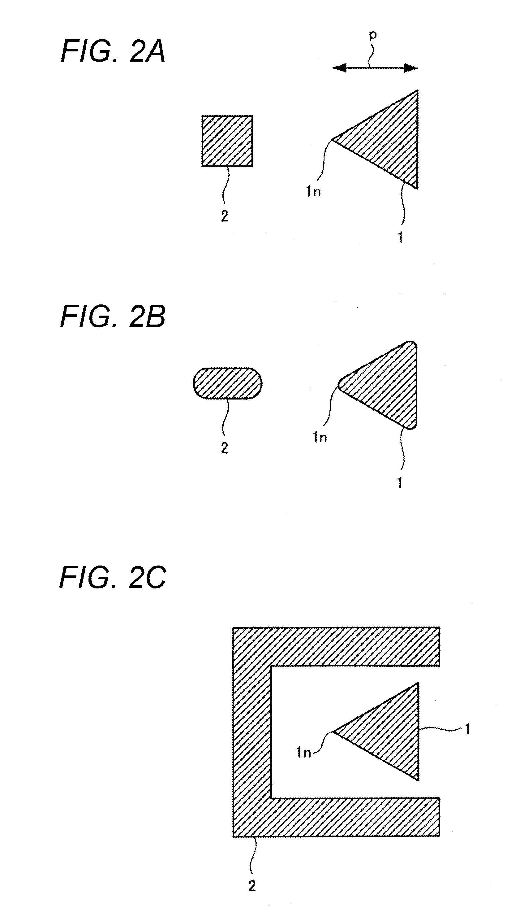
(1) Configuration of a Near-Field Light Generating Section

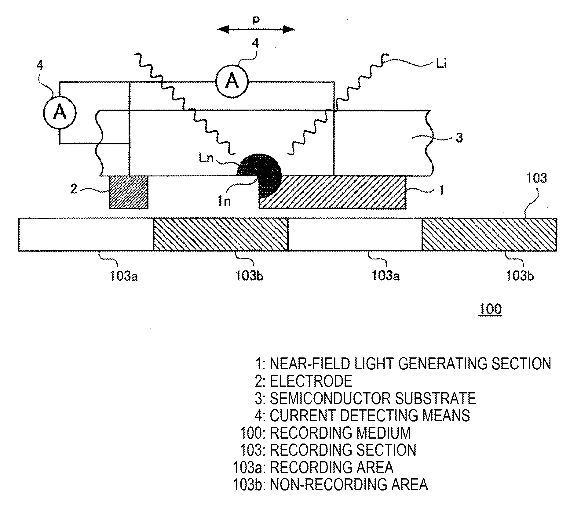
[0060]FIG. 1 is a diagram for explaining a signal detecting method according to a first embodiment of the present invention and is a schematic enlarged diagram of a main part of a signal detecting device according to this embodiment. In FIG. 1, a near-field light generating section 1 provided on a semiconductor substrate 3 of the signal detecting device is opposed to a recording section 103 of a recording medium 100. The near-field light generating section 1 and an electrode 2 are formed on the semiconductor substrate 3. A current detecting unit 4 is connected to the electrode 2. Incident light Li is irradiated from a not-shown light source. Near-field light is generated in a near-field light generation position in at one end of the near-field light generating section 1. The incident light Li is irradiated such that a field oscillation direction p thereof coincid...

second embodiment (

[2] Second Embodiment (Configuration of a Recording Medium)

[0090]It is expected to increase density in the phase change optical recording system by reproducing a recorded signal of, for example, the phase change recording medium 100 including the recording section made of the material, a dielectric constant of which changes, using the signal detecting device 50 according to the first embodiment. In the implementation of the increase in the density in the phase change optical recording system, improvement of a recording and reproduction characteristic can be expected according to contrivance explained below.

[0091]When a continuous film made of a phase change material is provided as the recording section 103 in the recording medium 100, the size of a recording mark is considered to depend on the size of a light spot. When the method of irradiating near-field light with the scatterer or the like is adopted even during recording, a near-field light field rapidly may decrease when the ne...


PUM

PropertyMeasurementUnit
wavelength bandaaaaaaaaaa
aspect ratioaaaaaaaaaa

Abstract

A signal detecting device includes: a semiconductor substrate; a near-field light generating section that is provided on the semiconductor substrate and generates near-field light near an interface with the semiconductor substrate; a light source that outputs light having wavelength corresponding to photon energy about a half as large as band-gap energy of a material of the semiconductor substrate; and a current detecting unit that detects a photocurrent generated in the semiconductor substrate when the near-field light is generated.

Description

BACKGROUND OF THE INVENTION[0001]1. Field of the Invention[0002]The present invention relates to a signal detecting device and a signal detecting method for detecting a signal recorded on a recording medium using near-field light.[0003]2. Description of the Related Art[0004]A light recording and reproducing method employing near-field light attracts attention as a technique for realizing an ultra-high density storage because the technique can realize high resolution regarded as a limit of a normal optical system. For example, when a so-called near-field light lens such as a solid immersion lens (SIL) is used, it is considered possible to reduce a spot diameter up to about 100 nm.[0005]It is expected that surface recording density 1 Tbit / inch2 will be realized in a hard disk around the year of 2012. However, to realize recording density equivalent to the surface recording density, it is necessary to set a spot diameter to be equal to or smaller than 20 nm.[0006]Therefore, in order to...

Claims


Application Information

Patent Timeline
Patent Type & Authority Applications(United States)
IPC IPC(8): G11B11/00
CPCB82Y10/00G11B2007/24328G11B7/005G11B7/007G11B7/1387G11B7/24035G11B7/24047G11B7/243G11B7/266G11B2007/24304G11B2007/24306G11B2007/2431G11B2007/24312G11B2007/2432G11B2007/24322G11B2007/24324G11B7/00454G11B9/12G11B13/08G11B11/24H01L31/108
Inventor NAKAOKI, ARIYOSHIKOJIMA, NAOTOSEKIGUCHI, KOJIKAWAKUBO, OSAMUFUJIIE, KAZUHIKO
Owner SONY CORP
Why Eureka
Try Eureka