Method for producing silicon substrate for solar cells

a technology of solar cells and silicon substrates, applied in semiconductor/solid-state device manufacturing, electrical equipment, semiconductors, etc., can solve the problems of poor surface passivation, high absorption coefficient of short-wavelength photons, and inability to meet multi-crystalline wafers, etc., to achieve suitable surface morphology and optical properties of silicon substrates.

Active Publication Date: 2009-12-17
IND TECH RES INST
View PDF3 Cites 22 Cited by
  • Summary
  • Abstract
  • Description
  • Claims
  • Application Information

AI Technical Summary

Benefits of technology

[0009]Accordingly, the present invention is directed to a method for producing a silicon substrate for solar cells, which can easily achieve the surface morphology and optical properties required by a multicrystalline silicon substrate.
[0011]In the present invention, the electroless wet chemistry technique using the aqueous solution is adopted during the whole producing process, and through performing the simple and robustly developed metal-activated selective oxidation and etching process, the suitable surface morphology and optical properties of the silicon substrate may be respectively obtained through using the selective oxidation solution composition, and through controlling the type of the oxidant as well as the etching time.

Problems solved by technology

Although the above method is an elegant and effective method for forming the surface texture of the mono-crystalline wafer, it is not suitable for the multicrystalline wafer, since the grains have different orientations.
That's because the porous silicon etching may result in poor surface passivation and high absorption coefficient for short wavelength photons.
Furthermore, as the direct band-gap behavior of the short wavelength response is reduced, the porous silicon layer has a appreciable absorption loss.
However, it is quite complicated to control the thickness of the metal-containing layer in terms of a large surface area.

Method used


Image

  • Method for producing silicon substrate for solar cells
  • Method for producing silicon substrate for solar cells
  • Method for producing silicon substrate for solar cells

Examples


example 1

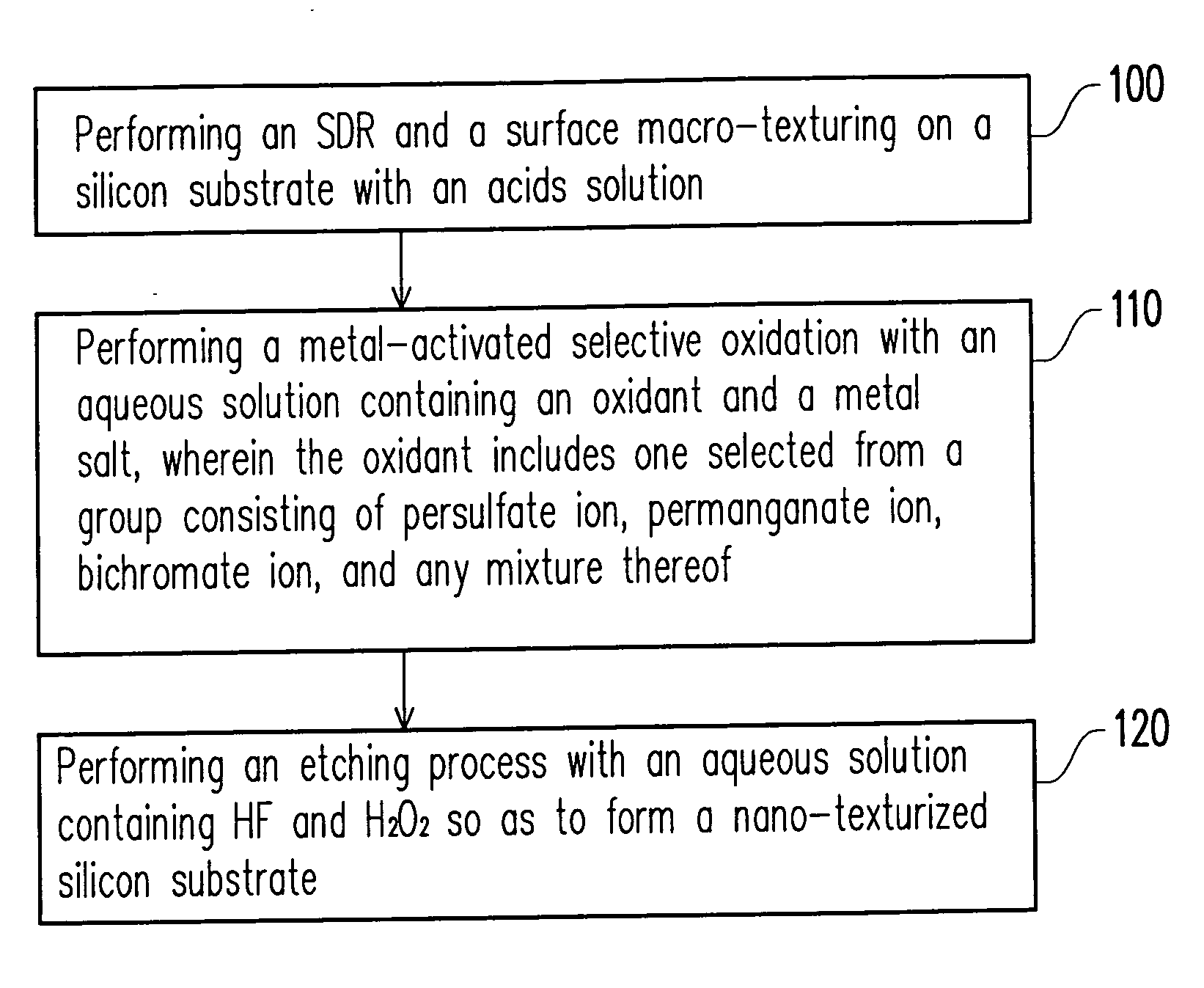
[0034]As-cut multicrystalline silicon substrates are rinsed with acetone and methanol or through a Piranha process. Then, the silicon substrates are etched for about 3 minutes under a temperature of 5-8° C. through using a solution of HF:HNO3:H2O at a volume ratio of 2.5:1:2.5, so as to perform the SDR and surface macro-texturing. Then, the silicon substrates are shortly immersed in a solution of KOH:H2O at a volume ratio of 1:50, so as to remove the formed nano-porous silicon layer. Then, the silicon substrates are rinsed with deionized water and then dried in a N2 flow.

[0035]Thereafter, the silicon substrates are first dipped in HF for 2-3 minutes in order to remove the native oxide layer, and then the metal-activated selective oxidation is performed. The metal-activated selective oxidation is performed by putting the silicon substrate into a solution of 0.1 M Na2S2O8 and 0.1 M AgNO3 at a volume ratio of 2:1 while stirring mildly at room temperature. The duration of the whole meta...

example 2

[0039]The pre-treatments in Table 1 are respectively performed on different multicrystalline silicon substrates.

TABLE 1SDRPolishingHF:HNO3:H2O = 2.5:1:2.5HF:HNO3 = 1:255-8° C., 3 minutes3-5 minutes, at room temperature

[0040]Then, the silicon substrates after being processed by different pre-treatments are soaked in HF for 2-3 minutes, for removing the native oxide layer, and then the silicon substrates are macro-texturized or polished. Then, the metal-activated selective oxidation is performed by putting the silicon substrates into the solution of 0.1 M Na2S2O8 and 0.1 M AgNO3 at a volume ratio of 5:1 at room temperature under agitation. The whole metal-activated selective oxidation is finished after approximately 5 minutes, and then the silicon substrates are rinsed with deionized water and then dried in the N2 flow.

[0041]Afterwards, the silicon substrates after the oxidation are put into the aqueous solution containing HF and H2O2 (the volume ratio of HF:H2O2:H2O is 1:5:10), and t...

example 3

[0043]The multicrystalline silicon substrates are produced through the manner of Example 1, but in the metal-activated selective oxidation process, Na2S2O8 and AgNO3 at the volume ratio of 10:1 is used.

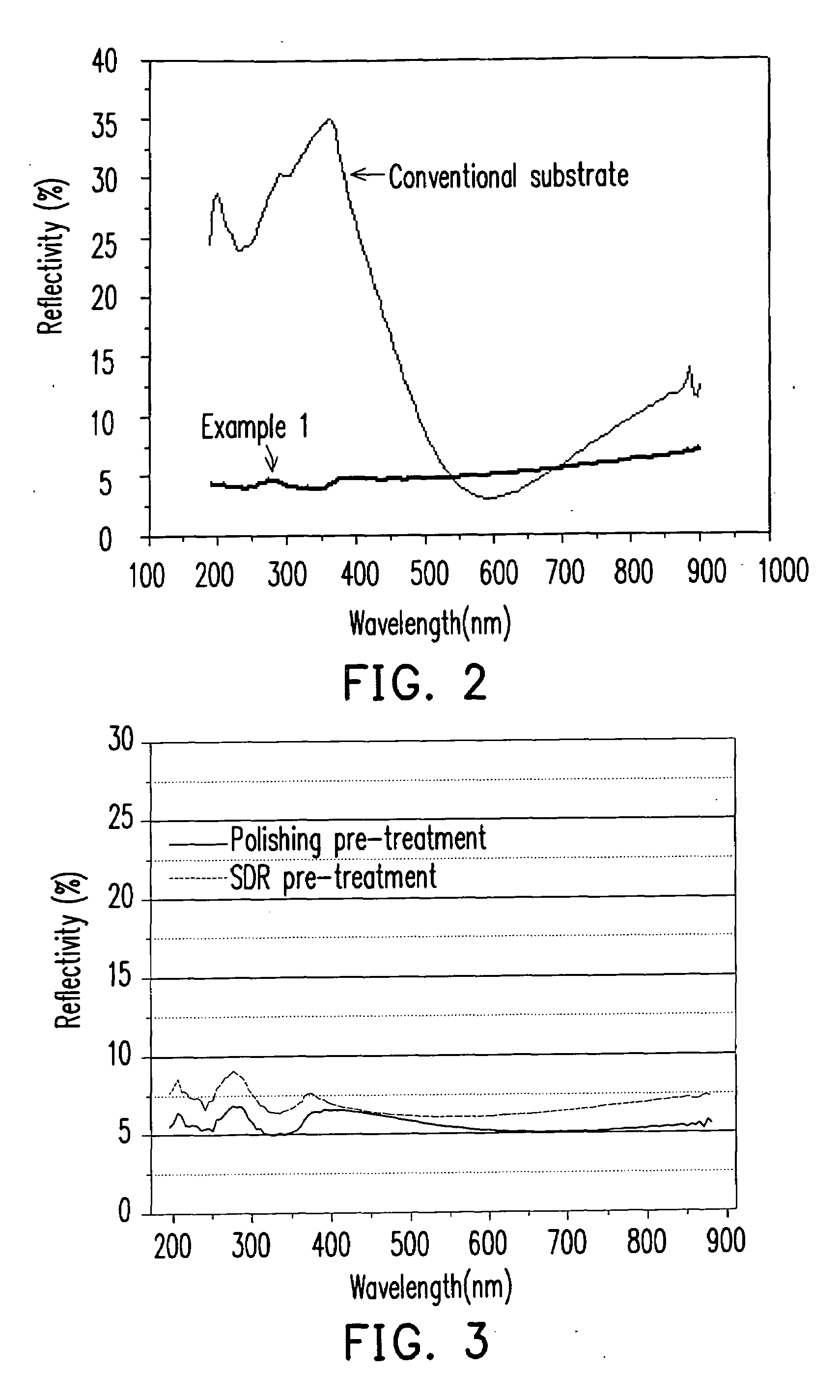
[0044]FIG. 4A is a graphical plot of reflectivity vs. wavelength after merely the SDR and the macro-texturing step are finished and after the nano-porous silicon layer is removed, and FIG. 4B is a graphical plot of reflectivity to wavelength after finishing all the steps. As can be known by comparing FIG. 4A with FIG. 4B that, only after the metal-activated selective oxidation and the etching process are performed on the silicon substrates, the reflectivity suppression effect can be achieved in the whole measured interval of wavelengths. FIGS. 5A and 5B are respectively SEM pictures of the surface of the silicon substrate at the stages of FIGS. 4A and 4B.

[0045]To sum up, in the present invention, the reflectivity can be easily reduced through a procedure consisting of as simple proces...


PUM


Abstract

A method for producing a silicon substrate for solar cells is provided. The method includes performing a saw damage removal (SDR) and surface macro-texturing on a silicon substrate with acids solution, so that a surface of the silicon substrate becomes an irregular surface. Thereafter, a metal-activated selective oxidation is performed on the irregular surface with an aqueous solution containing an oxidant and a metal salt, in which the oxidant is one selected from persulfate ion, permanganate ion, bichromate ion, and a mixture thereof. Afterwards, the irregular surface is etched with an aqueous solution containing HF and H2O2 so as to form a nano-texturized silicon substrate.

Description

BACKGROUND OF THE INVENTION[0001]1. Field of the Invention[0002]The present invention generally relates to a method for producing a silicon substrate for solar cells.[0003]2. Description of Related Art[0004]Solar cell is a very promising clean energy source, which can generate electricity directly from sunlights. However, the cost of the production of solar cells needs to be significantly reduced, so that the solar cells can be widely accepted as a major electricity source. Study shows that the silicon wafer share occupies over one third of the total cost of a crystal silicon (c-Si) solar cell module. Consequently, in order to reduce the cost, it has become an important development trend to make solar cells by multicrystalline silicon (mc-silicon) thin film.[0005]Recently, all high-efficiency mono-crystalline silicon solar cells have a particular textured structure on the front surface, so as to reduce the reflection loss and to improve the light-trapping property. Currently, the mo...

Claims


Application Information

Patent Timeline
Patent Type & Authority Applications(United States)
IPC IPC(8): H01L31/0236
CPCH01L31/02168Y02E10/50H01L31/0236H01L31/02363
Inventor DIMITROV, ZAHARIEVHUANG, CHIEN-RONGLIN, CHING-HSI
Owner IND TECH RES INST
Why Eureka
Try Eureka