Trench mosfet with shallow trench for gate charge reduction

a technology of trench mosfet and trench mosfet, which is applied in the direction of basic electric elements, electrical equipment, semiconductor devices, etc., can solve the problems of high gate charge, parasitically increasing rds, and shortage of tungsten plugs in the gate contact trench to the epitaxial layer, etc., to achieve the effect of reducing gate charg

Inactive Publication Date: 2009-12-24
FORCE MOS TECH CO LTD
View PDF7 Cites 32 Cited by
  • Summary
  • Abstract
  • Description
  • Claims
  • Application Information

AI Technical Summary

Benefits of technology

[0010]Another aspect of the present invention is that, the bottom of the trench is designed to be arc instead of rectangular, by using of this method, the density of electrical field around the bottom of the trench is lower than the prior art, as the art bottom reduces the curvature. And the most important is the breakdown voltage will not be decreased due to strong electrical field. Another advantage of using the arc bottom is that, when connecting trench is etched, it is easy to penetrate into the epitaxial layer through gate oxide when rectangular bottom is applied, which will lead to the shortage of tungsten plug to epitaxial layer, which means the design of arc trench bottom can partly avoid the chance of shortage. And in another embodiment, this problem could be prevented by forming a terrace poly, as will be discussed below.

Problems solved by technology

Conventional technology of forming trenched gate in the power MOS element is encountering a technical difficulty of high gate charge.
On the other hand, when etching the gate contact trench during fabricating process, it is possible to over etched to penetrate through the gate oxide and result in a shortage of tungsten plug filled in the gate contact trench to the epitaxial layer.
One problem is that, for the purpose of reducing the gate charge, the trench is not etched to a deep depth, and the difference between trench depth and P− body depth is therefore not large, which will parasitically increase Rds according to FIG. 2.
Another constraint is that, during the fabricating process, the gate contact trench is etched through an insulating layer and extending into trench filled material, since the distance left is so small and there is no any buffer layer, it could happen that the gate contact trench is over etched through gate oxide and lead to a shortage of tungsten plug filled in the gate contact trench and epitaxial layer.

Method used


Image

  • Trench mosfet with shallow trench for gate charge reduction
  • Trench mosfet with shallow trench for gate charge reduction
  • Trench mosfet with shallow trench for gate charge reduction

Examples


Embodiment Construction

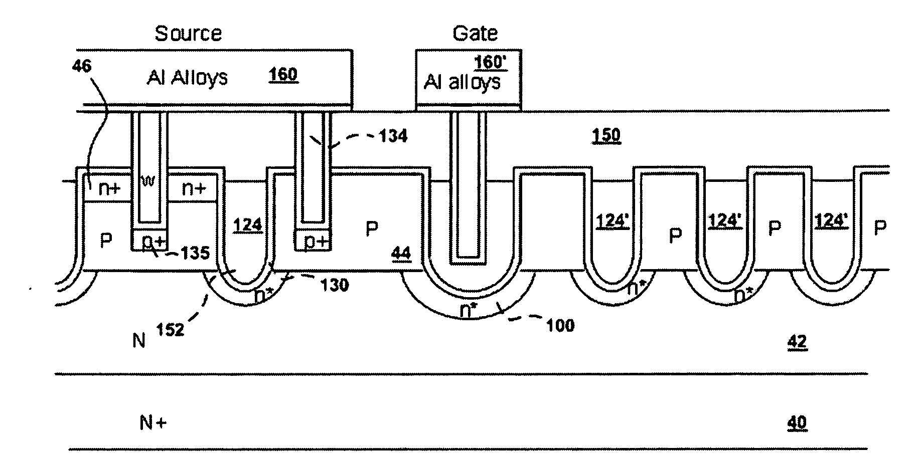
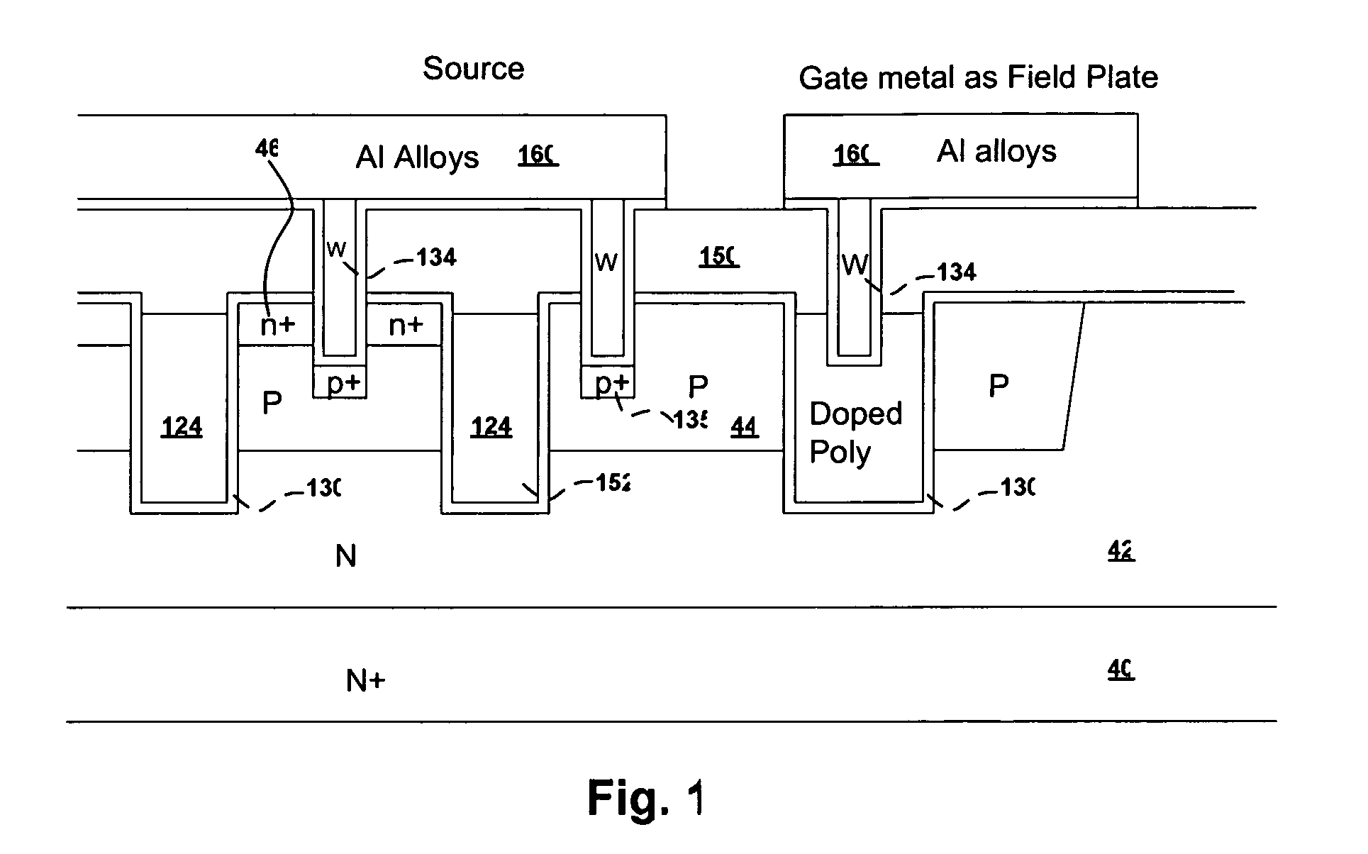
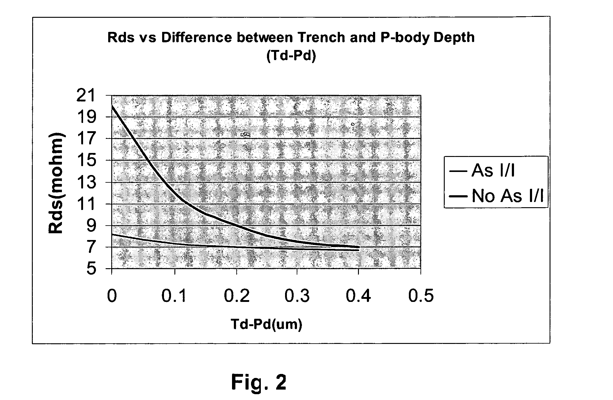
[0025]Please refer to FIG. 6 for an preferred embodiment of this invention where a power MOS element is formed on a red phosphorus N+ substrate 40, onto which formed an N epitaxial layer 42. The power MOS element further includes a trenched gate 124 disposed in a trench 124 with a gate insulation layer 130 formed over the walls of the trench. A body region 44 that is doped with a dopant of second conductivity type, e.g., P-type dopant, extends between the trenched gates. Trenches 124′ serves as floating trench rings as termination, and among all trenches, the trench for gate metal contact is wider than other else. It should be noticed that, the bottom of each trench, as shown in FIG. 6, is designed to be arc to form shallow trench for further reducing gate charge. Around said trench bottom, an N* region 100 is formed by arsenic Ion Implantation to further reduce Rds caused by decreasing the trench depth. Source region 46 doped with a first doping type is formed on the top surface of...


PUM


Abstract

A power MOS device includes shallow trench structure for reduction of gate charge. To counteract the increase of Rds may caused by decreasing the depth of trench, the power MOS device further includes an arsenic Ion Implantation area underneath each trench bottom when N+ red phosphorus substrate is applied, and the concentration of said arsenic doped area is higher than that of epitaxial layer. As the shallow trench is performed, the gate contact trench could be easily etched over to penetrate the gate oxide, which will lead to a shortage of tungsten plug filled in gate contact trench to epitaixial layer. To prevent from this problem, a terrace poly gate is designed in a preferred embodiment of present invention. By using this method, the gate contact trench is lifted to avoid the shortage problem.

Description

FIELD OF THE INVENTION[0001]This invention relates generally to the cell design and fabrication process of trench MOSFET devices. More particularly, this invention relates to a novel and improved cell structure and improved process of fabricating a trenched semiconductor power device with reduced drain-source resistance and reduced gate charge, as well as reduced cost.BACKGROUND[0002]Conventional technology of forming trenched gate in the power MOS element is encountering a technical difficulty of high gate charge. Only shallow the trench depth may lead to a increase of Rds while the conventional rectangular trench bottom may further decrease breakdown voltage as the electrical field density is high around rectangular trench bottom. On the other hand, when etching the gate contact trench during fabricating process, it is possible to over etched to penetrate through the gate oxide and result in a shortage of tungsten plug filled in the gate contact trench to the epitaxial layer.[0003...

Claims


Application Information

Patent Timeline
Patent Type & Authority Applications(United States)
IPC IPC(8): H01L29/78
CPCH01L29/0878H01L29/407H01L29/41766H01L29/4236H01L29/42372H01L29/7813H01L29/456H01L29/4925H01L29/66727H01L29/66734H01L29/7811H01L29/42376
Inventor HSIEH, FU-YUAN
Owner FORCE MOS TECH CO LTD
Why Eureka
Try Eureka