Variable gain current input amplifier and method

a voltage regulator and input amplifier technology, applied in the direction of dc-amplifiers with dc-coupled stages, differential amplifiers, amplifiers with semiconductor devices/discharge tubes, etc., can solve the problem that the topologies of ldo voltage regulators do not provide a sufficiently fast transient response to supply, the current consumption of some state-of-the-art digital logic circuit cells with advanced power saving features, etc., to achieve the effect of increasing the bandwidth of voltage regulator

Active Publication Date: 2009-12-31
TEXAS INSTR INC
View PDF0 Cites 61 Cited by
  • Summary
  • Abstract
  • Description
  • Claims
  • Application Information

AI Technical Summary

Benefits of technology

[0017]It is an object of the invention to provide LDO voltage regulator circuitry which can provide substantially increased voltage regulator bandwidth and large slewing current without stability problems without correspondingly increased power consumption and also without stability problems.
[0018]It is another object of the invention to provide LDO voltage regulator circuitry which can provide a very fast, large-swing drive signal to the gate of an output transistor of the LDO voltage regulator circuitry in response to a step-current increase in the current demanded by a load to thereby provide a large slewing current without substantially increasing the quiescent current of the voltage regulator and without causing stability problems.
[0019]It is another object of the invention to provide a variable gain amplifier which provides low gain under normal, non-slewing operating conditions and provides high gain under slewing conditions.
[0020]It is another object of the invention to provide LDO voltage regulator circuitry including a variable gain error amplifier which provides low gain under normal, non-slewing operating conditions and provides high gain under slewing conditions and enables the LDO voltage regulator circuitry to provide a very fast, large-swing drive signal to the gate of an output transistor of the LDO voltage regulator circuitry in response to a step-current increase in the current demanded by a load to thereby provide a large slewing current without substantially increasing the quiescent current of the voltage regulator and without causing stability problems.
[0021]It is another object of the invention to provide an improved, more easily implementable operational amplifier having a high slew rate.

Problems solved by technology

Unfortunately, current consumption of some state-of-the-art digital logic circuit cells with advanced power savings features that are fabricated using state-of-the-art processes can instantly (i.e., within a few picoseconds) vary from zero to a high maximum value.
Existing circuit topologies of LDO voltage regulators do not provide sufficiently fast transient response to supply the required load current steps, i.e., they are not capable of supplying such fast load current steps without the assistance of large load bypass capacitors.
Existing topologies of LDO voltage regulator circuits do not allow sufficiently fast transient response to supply such large instantaneous increases (i.e., steps) in the amount of demanded load current without using large external load bypass capacitors that have large capacitances (in the microfarad range) connected between the output of the LDO voltage regulator and a ground supply voltage.
As a practical matter, such large load bypass capacitors can not be included in an integrated circuit chip.
Although small load bypass capacitors having capacitances of up to a few nanofarads have indeed been included in digital logic circuit cells, such small load bypass capacitors are incapable of supplying large load instantaneous current steps and maintaining the precise voltage regulation needed by the digital logic circuit cells.
Use of large external load bypass capacitors adds substantial cost, including the cost of the capacitors themselves, the cost of extra package pins, and the cost of the die area of the required associated bonding pads.
This can make reliable operation of the digital logic cells nearly impossible.
The LDO voltage regulator circuitry provides large achievable small-signal bandwidth for a specified amount of current consumption and in a particular integrated circuit manufacturing process, but can not provide the fast large-signal load step response from loads the size of which range from very small load currents to very large load currents.
The circuit structure of prior art LDO voltage regulator 1 provides a large achievable small-signal bandwidth for a chosen total current consumption and a chosen integrated circuit manufacturing process, but can not provide a suitably fast large-signal response to a step increase in the current demanded by load 7 connected to the regulated output voltage Vout on conductor 6.
Consequently, the amount of current I1 of current source 11 must be substantially increased in order to achieve a correspondingly faster response of LDO voltage regulator 1 to a step increase in the demanded load current, thereby undesirably increasing the power consumption of prior art LDO voltage regulator 1.
The LDO voltage regulator of FIG. 2, which is taken from the foregoing patent application, partially solves the foregoing problems but was found to have stability problems.

Method used


Image

  • Variable gain current input amplifier and method
  • Variable gain current input amplifier and method
  • Variable gain current input amplifier and method

Examples


Embodiment Construction

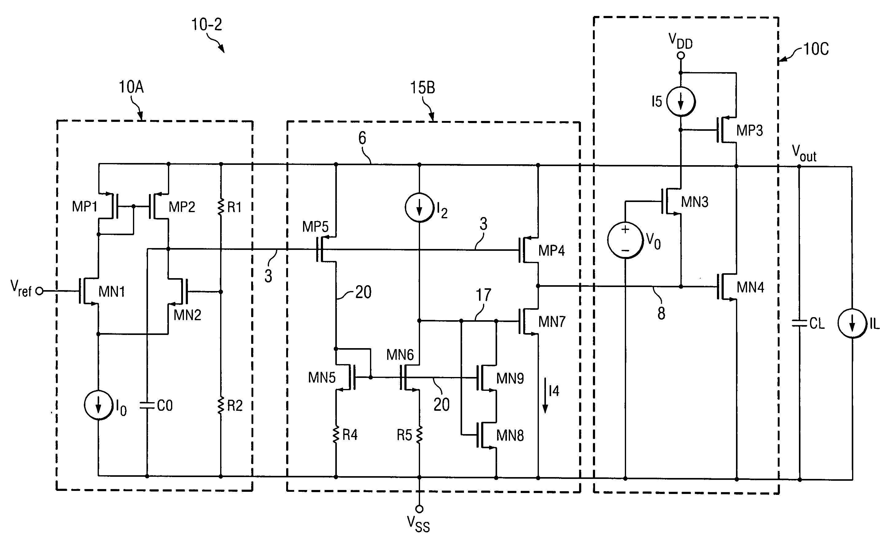
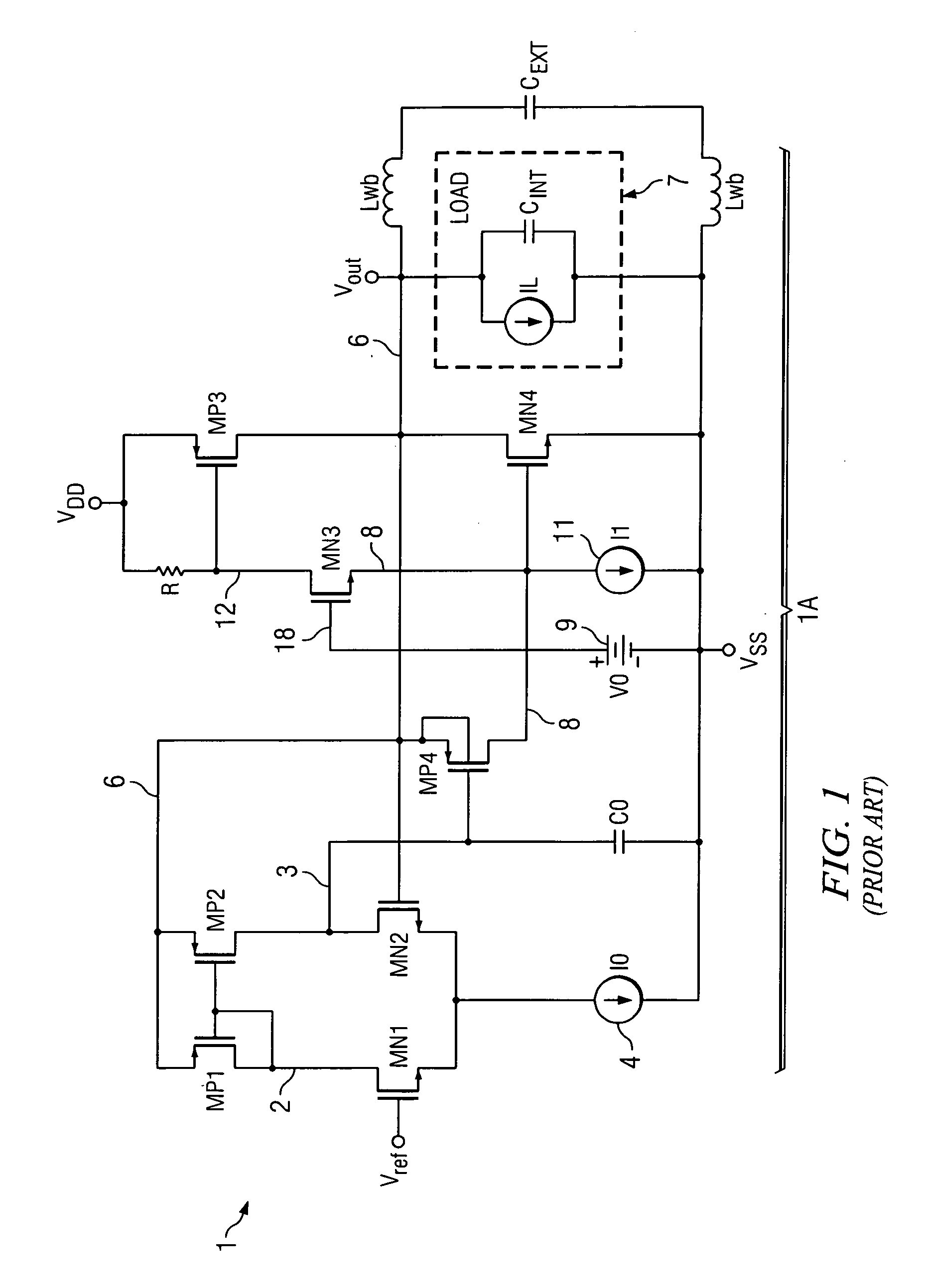
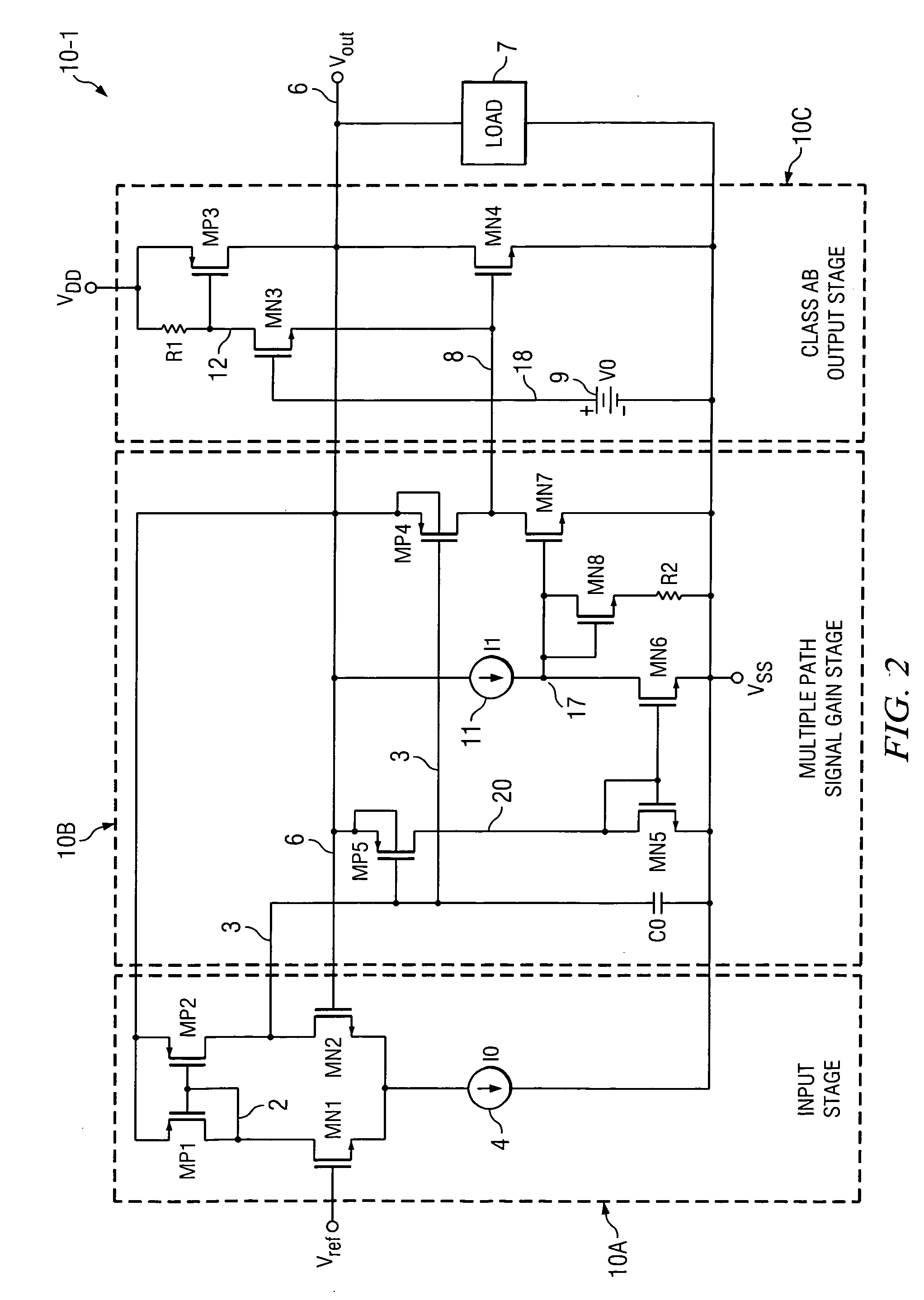
[0044]A solution to the above described problems of avoiding use of external load bypass capacitors and avoiding the associated voltage drops across parasitic wire bond inductances is the development of “embedded” on-chip LDO voltage regulators capable of responses to large, instantaneous large step changes in demanded load current which are much faster (e.g., 1-5 nanoseconds) than has previously been achievable.

[0045]To this end, and also to the end of providing improved slew boost in operational amplifiers, the present invention provides a new variable gain amplifier. Use of the variable gain amplifier in accordance with the present invention provides an operational amplifier having very fast, symmetrical slewing and settling, and also provides very fast response to large step changes in demanded load current and also provides very stable circuit operation. The invention also provides a low-dropout voltage regulator which includes the variable gain amplifier in the error amplifier...


PUM


Abstract

Variable gain circuitry includes a first input transistor (M1) having a source coupled to a first conductor (32), a gate coupled to a first input voltage (Vin+), and a drain coupled to a second conductor (30). An input of a first current mirror (M3,M4) is coupled to the second conductor to receive a current corresponding to the difference between the first input voltage and a second input voltage (Vin−). An output of the first current mirror is coupled to a source of current (M2). A first transistor (M5) has a gate coupled to a third conductor (31), a source coupled to a reference voltage (VSS), and a drain coupled to conduct output current (Iout). A second transistor (M6) and a resistive element (M7) are coupled in series between the third conductor and the first reference voltage (VSS), a gate of the second transistor being coupled to the third conductor to produce a nonlinear relationship between currents of the first transistor and the second transistor.

Description

BACKGROUND OF THE INVENTION[0001]The present invention relates generally to variable gain amplifiers which are useful in various applications, especially as slew boost circuits for high slew rate operational amplifiers, and also in high bandwidth LDO voltage regulators that require improved transient response to instant increases (i.e. step increases) in demanded load current without use of large, external load bypass capacitors, particularly low-dropout voltage regulators (LDO voltage regulators) which are especially suited to being embedded in various integrated circuit chips that require precise internal load voltage regulation.[0002]The closest prior art related to operational amplifiers having high slew rates is believed to include commonly owned U.S. Pat. No. 6,437,645 entitled “Slew Rate Boost Circuitry and Method” issued to Ivanov et al. on Aug. 20, 2002. A main shortcoming of this prior art is that the common-mode input voltage can not go closer than 2 gate-to-source voltag...

Claims


Application Information

Patent Timeline
Patent Type & Authority Applications(United States)
IPC IPC(8): H03F3/45
CPCH03F3/45179H03F2203/45674H03F3/45183
Inventor IVANOV, VADIM V.KUNZ, KEITH E.BANDIGADI, SACHIN RAOMANGINA, PRASADU NAGA VENKATA
Owner TEXAS INSTR INC
Why Eureka
Try Eureka