Imaging system and method of driving the same
a technology of imaging system and driving mode, applied in the field of imaging system, can solve problems such as power consumption increase, and achieve the effect of increasing dynamic range and improving s/n ratio
- Summary
- Abstract
- Description
- Claims
- Application Information
AI Technical Summary
Benefits of technology
Problems solved by technology
Method used
Image

Examples
first embodiment
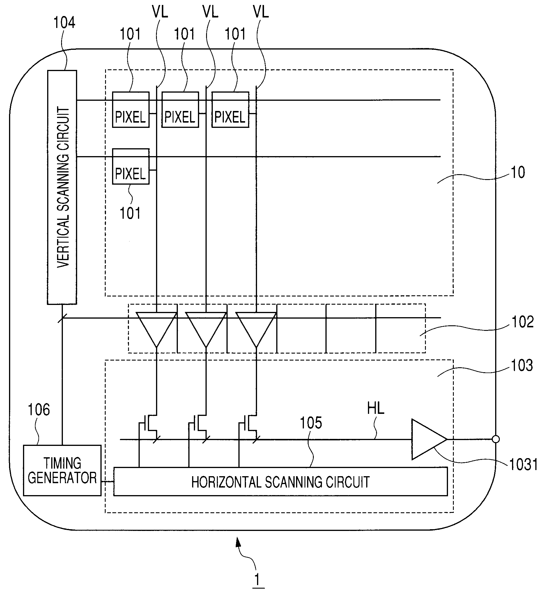
[0041]FIG. 3 is a schematic diagram illustrating an example of configuration of a solid-state imaging device according to the first embodiment of the present invention. The same components as those in FIG. 1 are denoted by the same reference numerals. The solid-state imaging device 1 includes a signal storage unit 107 in an output portion 103.
[0042]FIG. 4 is an equivalent circuit diagram illustrating more in detail the configuration including from a pixel 101 to an output amplifier 1031 in FIG. 3.
[0043]The pixel 101 includes a photodiode PD being a photoelectric conversion element and a transfer unit for transferring charges stored in the photodiode to the gate terminal of a MOS transistor forming a pixel output unit SF. The gate terminal being the input portion of the pixel output unit SF is connected to a power supply VDD through a reset portion RES. The source terminal of the pixel output unit SF is connected to one terminal of an input capacitor C0 of the column amplifier 102 vi...
second embodiment
[0086]The second embodiment of the present invention is described below with reference to FIG. 9. The present embodiment is different from the first embodiment in that a plurality of column amplifiers is provided for each column of a pixel.
[0087]FIG. 9 is a schematic diagram illustrating one pixel extracted from a column of pixels. The two column amplifiers 102-1 and 102-2 are provided on the vertical signal line VL. Herein, the input capacitors C0 of the column amplifiers 102-1 and 102-2 are the same in capacitance value. The column amplifiers 102-1 and 102-2 are different in that the capacitances of the feedback capacitors provided on the feedback paths between the inverting input terminal and the output terminal of the operational amplifier Amp are different from each other. The feedback capacitors C1 and C2 are connected to the column amplifier 102-1 and the feedback capacitors C3 and C4 are connected to the column amplifier 102-2. The capacitance values of the feedback capacito...
third embodiment
[0101]Another embodiment to which the present invention can be applied is described with reference to FIG. 11.
[0102]FIG. 11 is a schematic diagram illustrating a part of one column extracted from a pixel portion according to the present embodiment. Although four pixels are illustrated as one-column portion of the pixel portion, the present embodiment is not limited to this number. In the present embodiment, pixels including the photodiodes PD and the transfer portions TX are arranged in a matrix. By turning on the transfer portion TX in response to the signal φTX, charges stored in the photodiode PD are transferred to a vertical CCD circuit VCCD and the charges are sequentially transferred to a buffer unit buf in response to a vertical transfer pulse (not shown). The buffer unit buf is a charge-to-voltage converting portion for converting into a voltage a charge transferred from the vertical CCD circuit VCCD. The output of the buffer unit buf is input to the column amplifier 102. Th...
PUM
 Abstract
Description
Claims
Application Information
 - Generate Ideas
- Intellectual Property
- Life Sciences
- Materials
- Tech Scout
- Unparalleled Data Quality
- Higher Quality Content
- 60% Fewer Hallucinations
Browse by: Latest US Patents, China's latest patents, Technical Efficacy Thesaurus, Application Domain, Technology Topic, Popular Technical Reports.
© 2025 PatSnap. All rights reserved.Legal|Privacy policy|Modern Slavery Act Transparency Statement|Sitemap|About US| Contact US: help@patsnap.com