

Ozone and teos process for silicon oxide deposition
- Summary
- Abstract
- Description
- Claims
- Application Information
AI Technical Summary
Benefits of technology
Problems solved by technology
Method used
Image

Examples
example 1
[0059]Using TEOS and O2 as precursors, silicon oxide was formed on substrates containing trenches about 100 nm wide and having an aspect ratio of about 4. The deposition was performed in a A412™ batch reactor from ASM International N.V. of Bilthoven, The Netherlands. TEOS and oxygen were flowed into the reaction chamber of the reactor continuously and simultaneously, at a constant rate. TEOS was flowed at about 100 sccm and O2 was flowed at about 13 sccm. The substrate temperature was about 675° C. The reaction chamber pressure was about 250 mTorr. A total thickness of about 650 nm of silicon oxide was deposited.
[0060]The substrates were then annealed in two stages in an ASM A412™ wet oxide vertical furnace from ASM International N.V. of Bilthoven, The Netherlands. First, the substrates are annealed at 750° C. for 30 minutes in a steam atmosphere. Second, the substrates are annealed at 1050° C. for 30 minutes in a nitrogen atmosphere.
[0061]FIG. 10 illustrates the results of the depo...
example 2
[0062]Silicon oxide was deposited into trenches using TEOS and O3 as precursors flowed continuously and simultaneously into a reaction chamber at a constant rate. The trenches were about 100 nm wide, with an aspect ratio of about 4. The deposition was performed in a A412™ batch reactor from ASM International N.V. of Bilthoven, The Netherlands. TEOS and ozone were flowed into the reaction chamber. TEOS was flowed at about 450 sccm and ozone was flowed at about 0.15 slm. The substrate temperature was about 600° C. and the reaction chamber pressure was about 1500 mTorr. A total thickness of about 650 nm of silicon oxide was deposited.
[0063]The substrates were then annealed in two stages in an ASM A412™ wet oxide vertical furnace from ASM International N.V. of Bilthoven, The Netherlands. First, the substrates are annealed at 750° C. for 30 minutes in a steam atmosphere. Second, the substrates are annealed at 1050° C. for 30 minutes in a nitrogen atmosphere.
[0064]FIG. 11 illustrates the ...
example 3
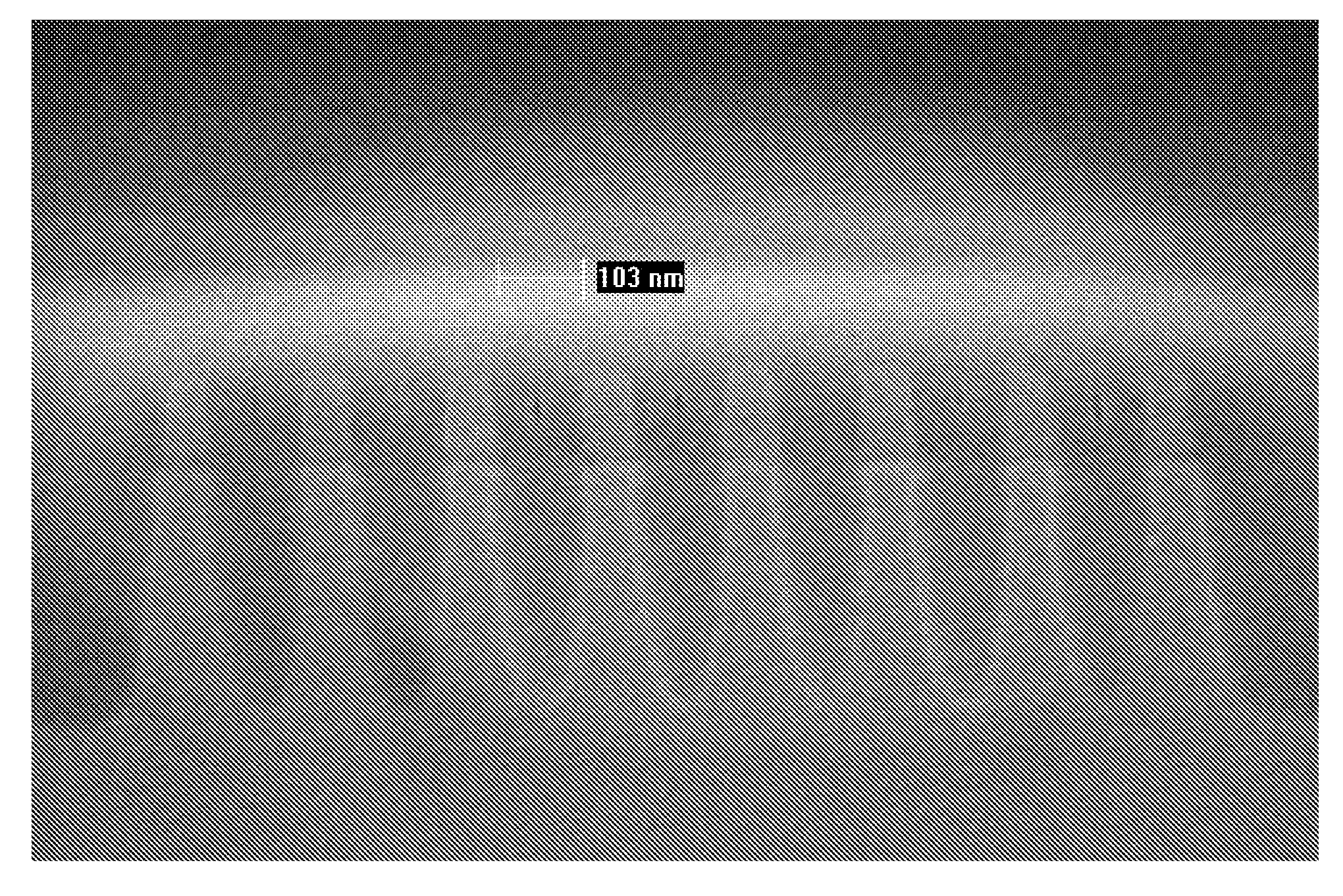
[0065]Silicon oxide was deposited into trenches using TEOS and O3 as precursors. The trenches were about 100 nm wide, with an aspect ratio of about 4. The deposition was performed in a A412™ batch reactor from ASM International N.V. of Bilthoven, The Netherlands. TEOS was pulsed and ozone was flowed continuously, at a fixed rate, into the reaction chamber. TEOS was pulsed at about 450 sccm (714 pulses) and ozone was flowed at about 2.5 slm. The substrate temperature was about 600° C. and the reaction chamber pressure was about 750 mTorr. About 650 nm of silicon oxide was deposited.
[0066]The substrates were then annealed in two stages in an ASM A412™ wet oxide vertical furnace from ASM International N.V. of Bilthoven, The Netherlands. First, the substrates are annealed at 750° C. for 30 minutes in a steam atmosphere. Second, the substrates are annealed at 1050° C. for 30 minutes in a nitrogen atmosphere.
[0067]FIG. 13 illustrates the results of the deposition. Advantageously, the occu...
PUM
| Property | Measurement | Unit |
|---|---|---|
| Pressure | aaaaa | aaaaa |
| Pressure | aaaaa | aaaaa |
| Pressure | aaaaa | aaaaa |
Abstract
Description
Claims
Application Information