Planar transmission line-to-waveguide transition apparatus and wireless communication module having the same

a transition apparatus and waveguide technology, applied in electrical devices, multiple-port networks, coupling devices, etc., can solve the problems of degrading the performance increasing the overall size of the wireless communication module, and small size, and achieves low insertion loss and large bandwidth.

Inactive Publication Date: 2010-01-07
KOREA ADVANCED INST OF SCI & TECH
View PDF5 Cites 13 Cited by
  • Summary
  • Abstract
  • Description
  • Claims
  • Application Information

AI Technical Summary

Benefits of technology

[0011]It is, therefore, an object of the present invention to provide a planar transmission line-to-waveguide transition apparatus havin...

Problems solved by technology

The biggest issue of the techniques is to develop small size, low cost wireless communication modules operating at millimeter-wave bands, and this may be achieved in general through the use of a system-in-package (SiP) technique.
However, when the antenna is installed at the same plane as a signal processing circuit, for example, a monolithic millimeter-wave integrated circuit (MMIC), the overall size of the wireless communication module increases and incomplete isolation between the antenna and the signal processing circuit is also likely to degrade the performance of the wireless communication module.
The transition apparatus disclosed in the article by Yusuke Deguchi et al. exhibits low loss wide-band characteristics but has shortcomings in that an upper waveguide has to be manufactured additionally through a mechanical process and ...

Method used


Image

  • Planar transmission line-to-waveguide transition apparatus and wireless communication module having the same
  • Planar transmission line-to-waveguide transition apparatus and wireless communication module having the same
  • Planar transmission line-to-waveguide transition apparatus and wireless communication module having the same

Examples


Embodiment Construction

[0033]Hereinafter, exemplary embodiments of the present invention will be described in detail with reference to the accompanying drawings.

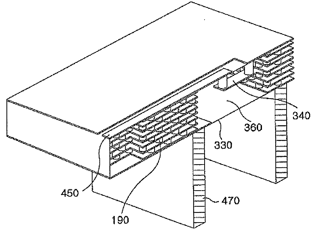
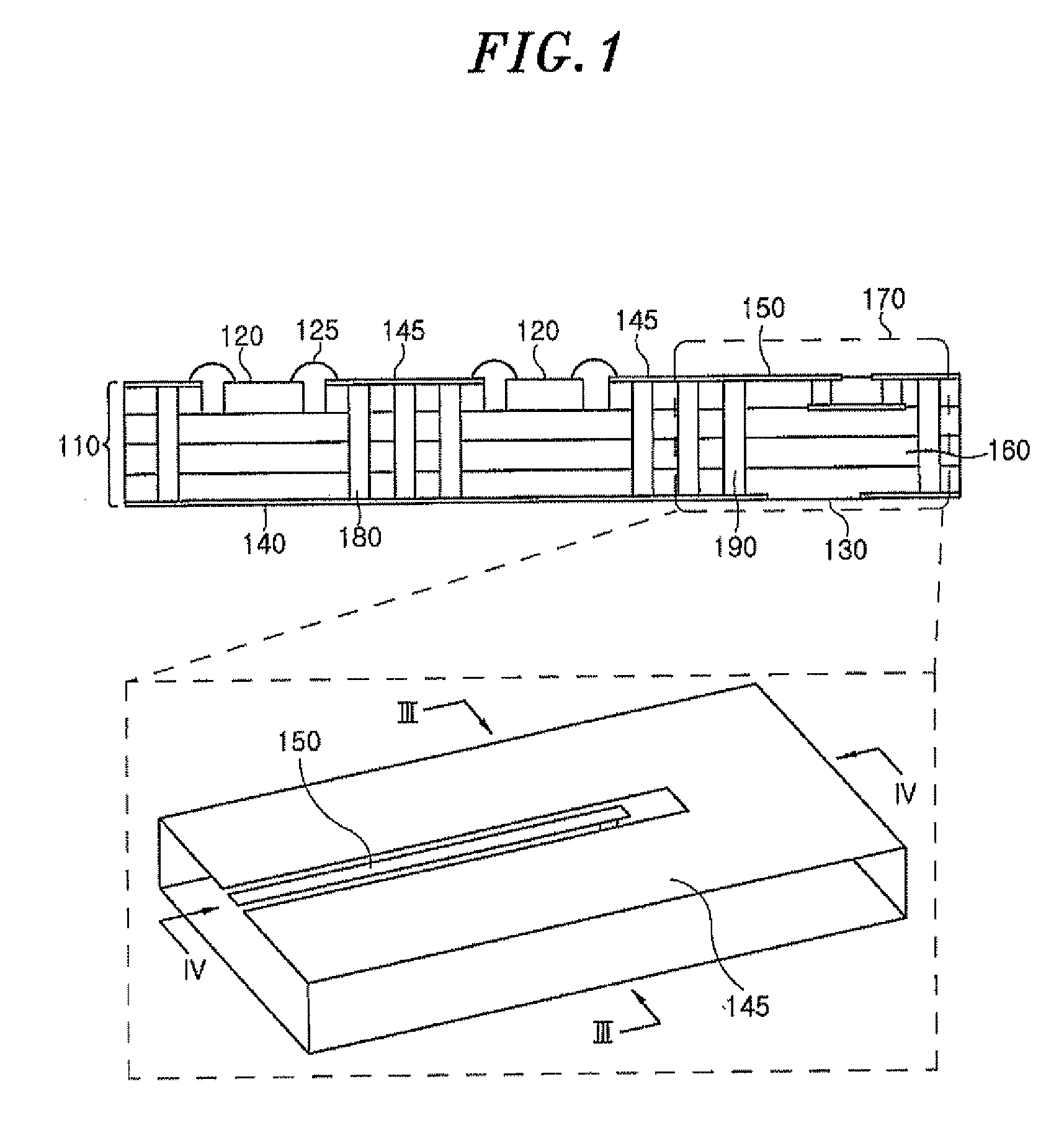
[0034]FIG. 1 shows a schematic view of a wireless communication module in accordance with the present invention, which includes a cross-sectional view of the wireless communication module having a built-in planar transmission line-to-waveguide transition apparatus, and an enlarged perspective view of the planar transmission line-to-waveguide transition apparatus.

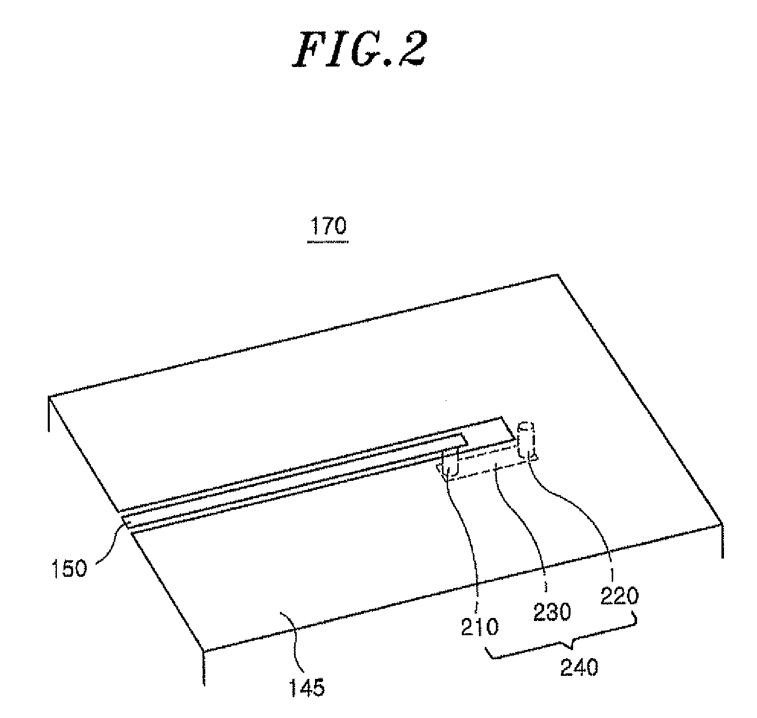
[0035]As shown in FIG. 1, a wireless communication module, which operates at millimeter-wave bands and is configured by a SiP technique, includes a multi-layer substrate 110 formed by using an LTCC (low temperature co-fired ceramic). The wireless communication module further includes plural MMICs 120 placed on the uppermost surface of the multi-layer substrate 110, and a planar transmission line 150 such as a microstrip line or a coplanar waveguide (CPW) formed for communications between t...


PUM


Abstract

A wireless communication module includes a plurality of monolithic millimeter-wave integrated circuits (MMICs) for signal processing attached to the top surface of a multi-layer low temperature co-fired ceramic substrate; a planar transmission line formed on the top surface of the multi-layer substrate for communications between the MMICs; a metal base attached to the bottom surface of the multi-layer substrate and having an opening to which an antenna is attached; a plurality of vias for connecting the metal base and the planar transmission line within the multi-layer substrate to establish a uniform potential on a ground plane of the multi-layer substrate; an embedded waveguide formed in the opening surrounded with the vias within the multi-layer substrate; and a planar transmission line-to-waveguide transition apparatus for the transition of waves between the planar transmission line and the embedded waveguide.

Description

FIELD OF THE INVENTION[0001]The present invention relates to wireless communication modules operating at millimeter-wave bands, and more specifically, to a wireless communication module having a built-in planar transmission line-to-waveguide transition apparatus.BACKGROUND OF THE INVENTION[0002]With exponential demand for the wireless communications of a high speed and large capacity, high-speed broadband wireless communication techniques have been required to meet such a demand and to process data at a rate of certain Gbps range. In recent, millimeter-wave band wireless communication modules having a wide bandwidth are drawn a lot of attention. The biggest issue of the techniques is to develop small size, low cost wireless communication modules operating at millimeter-wave bands, and this may be achieved in general through the use of a system-in-package (SiP) technique. In the SIP technique, an antenna is an absolute factor that determines the total size of a wireless communication...

Claims


Application Information

Patent Timeline
IPC IPC(8): H01P5/107
CPCH01P5/107
Inventor LEE, JAE JINPARK, CHUL SOONJUNG, DUNG YUNEUN, KI CHAN
Owner KOREA ADVANCED INST OF SCI & TECH
Why Eureka
Try Eureka