Condenser microphone and MEMS device

a condenser microphone and microphone technology, applied in the direction of microstructural devices, electrical transducers, transducer types, etc., can solve the problems of sticking between the stopper and the electrode opposed to the stopper, and the likelihood of sticking, so as to achieve good sticking resistance, good sticking resistance, good sticking resistance

Inactive Publication Date: 2010-01-07
PANASONIC CORP
View PDF9 Cites 44 Cited by
  • Summary
  • Abstract
  • Description
  • Claims
  • Application Information

AI Technical Summary

Benefits of technology

[0023]According to the MEMS device of the present invention, a recess is provided in the center of each stopper of the first film having the first electrode film. Hence, the contact area between the stopper and the second film can be reduced even when the first film and the second film come close to each other. Accordingly, a high-performance MEMS device good in sticking resistance can be implemented without the necessity of changing the stopper size even when the number of stoppers is increased.
[0024]According to the present invention, a high-performance MEMS device good in sticking resistance can be implemented without the necessity of changing the stopper size even when the number of stoppers is increased. Also, with good sticking resistance, the moisture resistance and condensation resistance of the MEMS device can be improved.
[0025]Also, according to the present invention, in formation of the air gap structure having a thickness of the order of several μm between the first film and the second film by wet etching, the contact area between the opposed films can be reduced even when the opposed films with the air gap therebetween are about to contact each other via a medium such as water and isopropyl alcohol (IPA). In other words, according to the present invention, a MEMS device capable of exerting strong sticking resistance even during fabrication can be implemented.

Problems solved by technology

However, the conventional stopper structures disclosed in Patent Documents 1 to 4 have a problem as follows.
An increased number of stoppers however may cause sticking between the stoppers and the electrode opposed to the stoppers.
Hence, sticking is likely to occur as the number of stoppers increases.

Method used


Image

  • Condenser microphone and MEMS device
  • Condenser microphone and MEMS device
  • Condenser microphone and MEMS device

Examples


embodiment 1

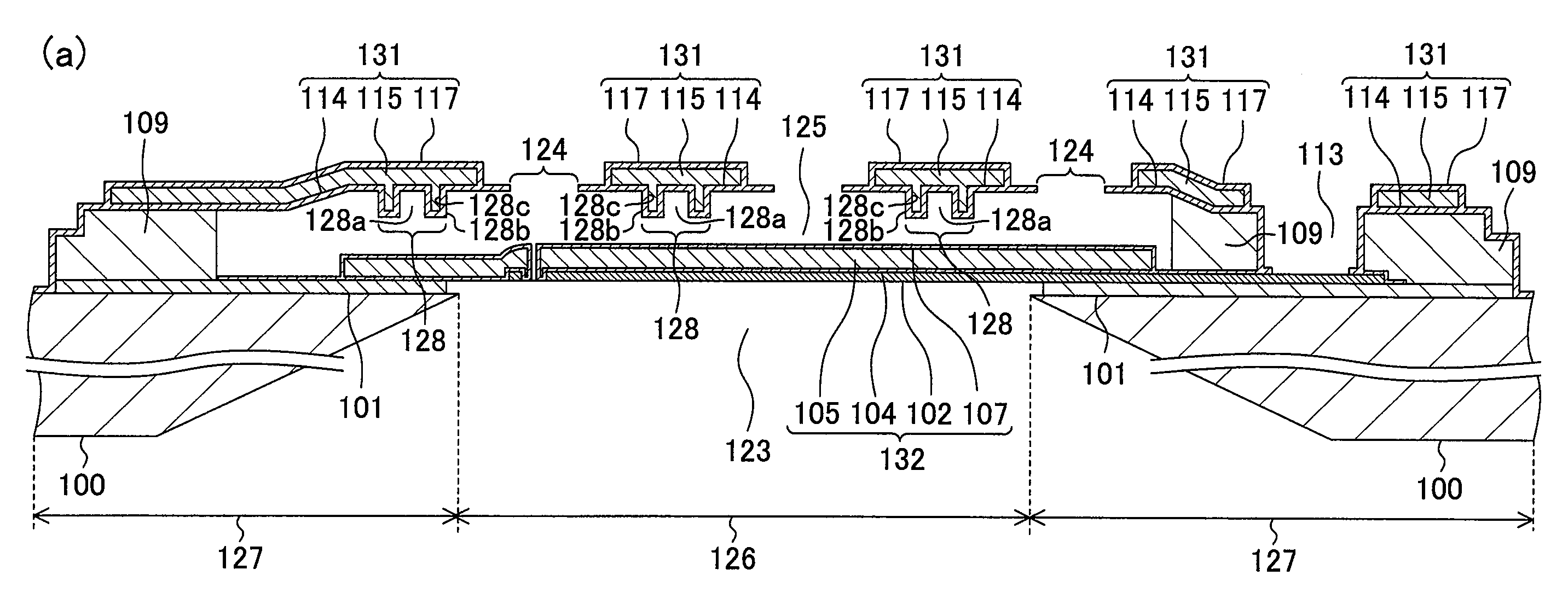
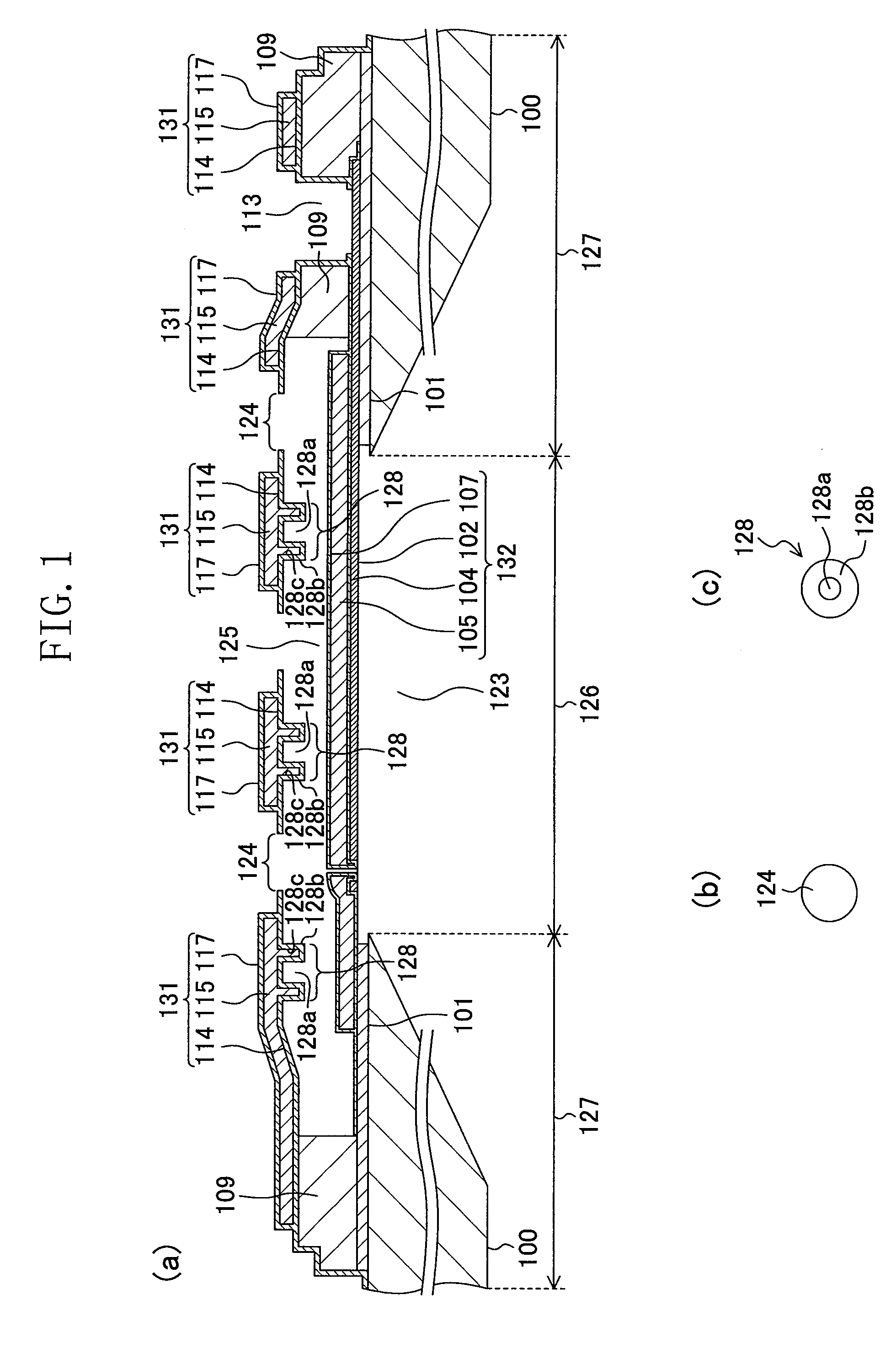
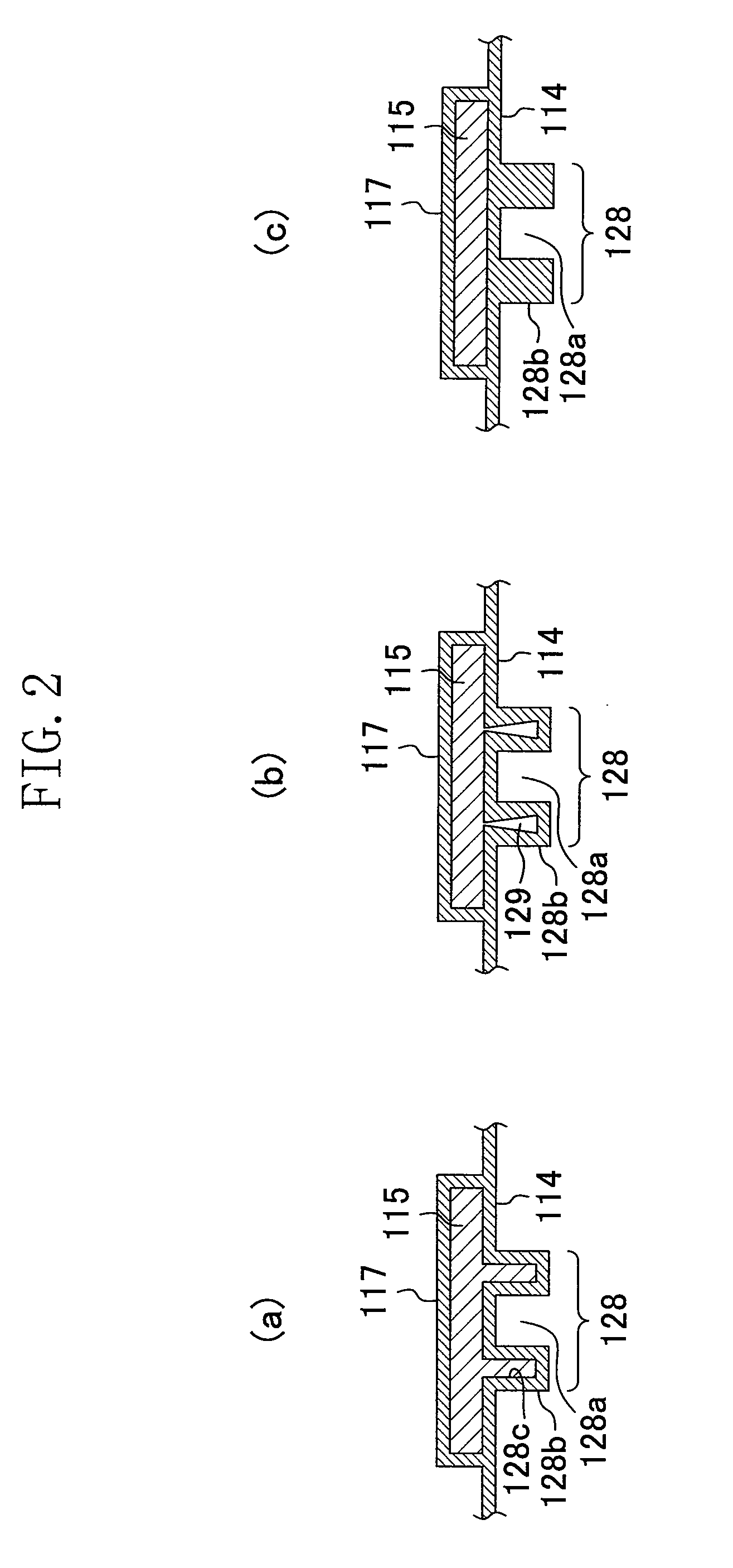
[0053]Hereinafter, a condenser microphone of Embodiment 1 of the present invention will be described with reference to FIGS. 1(a) to 1(c).

[0054]As shown in the cross-sectional view of FIG. 1(a), the condenser microphone of Embodiment 1 of the present invention includes a semiconductor substrate 100 having a substrate removed portion 123 in the center, or to state differently, a semiconductor substrate 100 having a membrane region 126 and a peripheral region 127 (part of the region outside the membrane region 126). As the semiconductor substrate 100, used is a silicon single crystal having a (100) principal plane and a specific resistance of 10 to 15 Ω·cm, for example. A protection oxide film (first silicon oxide film) 101 is formed on the peripheral region 127 of the semiconductor substrate 100. A multilayer film (second multilayer film) 132 made of a polysilicon film (first conductive polysilicon film) 102, a silicon nitride film (first silicon nitride film) 104, a silicon oxide fi...

embodiment 2

[0079]Hereinafter, a condenser microphone of Embodiment 2 of the present invention will be described with reference to FIGS. 10(a) to 10(c).

[0080]As shown in the cross-sectional view of FIG. 10(a), the condenser microphone of Embodiment 2 includes a semiconductor substrate 200 having a substrate removed portion 223 in the center, or to state differently, a semiconductor substrate 200 having a membrane region 226 and a peripheral region 227 (part of the region outside the membrane region 226). As the semiconductor substrate 200, used is a silicon single crystal having a (100) principal plane and a specific resistance of 10 to 15 Ω·cm, for example. A protection oxide film (first silicon oxide film) 201 is formed on the peripheral region 227 of the semiconductor substrate 100. A multilayer film (second multilayer film) 232 made of a polysilicon film (first conductive polysilicon film) 202, a silicon nitride film (first silicon nitride film) 204, a silicon oxide film (second silicon oxi...

embodiment 3

[0102]Hereinafter, a condenser microphone of Embodiment 3 of the present invention will be described with reference to FIGS. 18(a) to 18(c).

[0103]As shown in the cross-sectional view of FIG. 18(a), the condenser microphone of Embodiment 3 includes a semiconductor substrate 300 having a substrate removed portion 324 in the center, or to state differently, a semiconductor substrate 300 having a membrane region 327 and a peripheral region 328 (part of the region outside the membrane region 327). As the semiconductor substrate 300, used is a silicon single crystal having a (100) principal plane and a specific resistance of 10 to 15 Ω·cm, for example. A protection oxide film (first silicon oxide film) 301 is formed on the peripheral region 328 of the semiconductor substrate 300. A multilayer film (second multilayer film) 332 made of a polysilicon film (first conductive polysilicon film) 302, a silicon nitride film (first silicon nitride film) 304, a silicon oxide film (second silicon oxi...


PUM


Abstract

An air gap is formed between a first film having a first electrode film and a second film having a second electrode film. The first film has a stopper protruding toward the second film, and a recess communicating with the air gap is provided in the center of the stopper.

Description

[0001]This is a continuation of Application PCT / JP2009 / 000002, filed on Jan. 5, 2009.BACKGROUND OF THE INVENTION[0002]The present invention relates to a microelectromechanical systems (MEMS) device such as a condenser microphone having a vibrating electrode and a fixed electrode.[0003]In recent years, capacitive vibration sensors utilizing MEMS technology, as those disclosed in Patent Documents 1 and 2, have been proposed. The capacitive vibration sensors disclosed in Patent Documents 1 and 2 have a feature that a fixed electrode and a vibrating electrode are opposed to each other with an air gap (space) therebetween on a substrate and the fixed electrode has a stopper (protrusion). The stopper is provided for preventing the fixed electrode and the vibrating electrode from coming within a given distance of each other. Specifically, if condensation occurs in the air gap or a foreign matter such as water enters the air gap, the opposed fixed electrode and vibrating electrode may come ...

Claims


Application Information

Patent Timeline
Patent Type & Authority Applications(United States)
IPC IPC(8): H04R11/04H01L29/84
CPCB81B3/0051H04R19/016H01G7/02B81B2201/0257
Inventor NOTAKE, HIDENORIYAMAOKA, TOHRU
Owner PANASONIC CORP
Why Eureka
Try Eureka