Method for manufacturing image display device

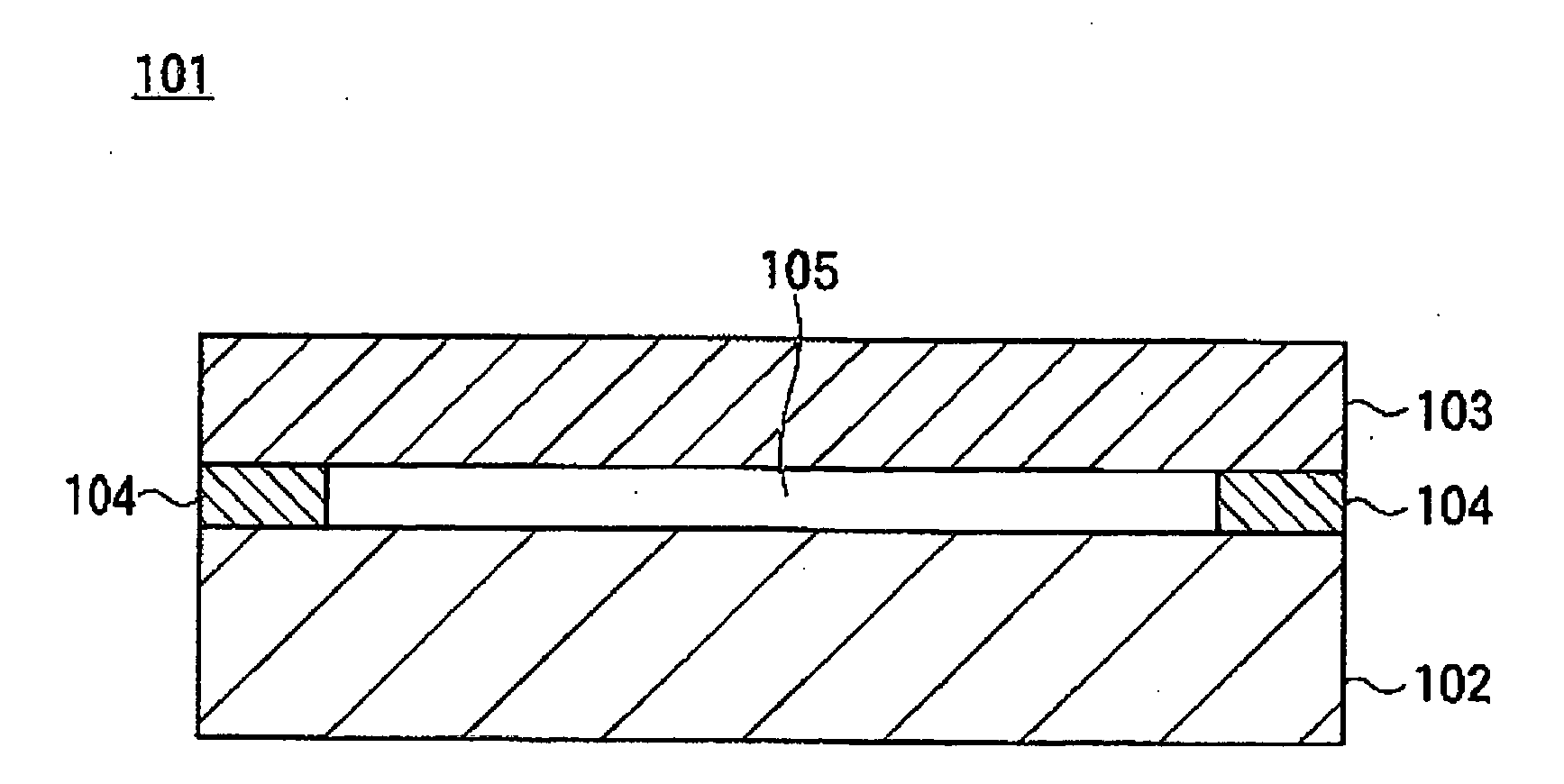
a technology of image display device and manufacturing method, which is applied in the direction of manufacturing tools, electric/magnetic/electromagnetic heating, instruments, etc., can solve the problems of display defects, deformation of optical glass, and gap 105, so as to reduce the amount of thermal polymerization initiator used, reduce the influence of heat on various plastic materials used near the image display device, and reduce the effect of cured

Active Publication Date: 2010-01-07
DEXERIALS CORP
View PDF6 Cites 77 Cited by
  • Summary
  • Abstract
  • Description
  • Claims
  • Application Information

AI Technical Summary

Benefits of technology

[0017]In the present invention, a photo-curable resin composition is interposed between the base including the image display unit and the light-transmitting protection member including the light-shielding member and is photo-cured to form a cured resin layer. The present invention includes the step of interposing a curable resin composition containing a thermal polymerization initiator at least between the light-shielding member and the base and then heating the curable resin composition. Therefore, the resin composition can be sufficiently cured even in the area where the light-shielding member is formed.
[0018]In the present invention, the photo-curable resin composition interposed between a non-light-shielding portion and the base may not contain a thermal polymerization initiator, and the photo-curable resin composition containing the thermal polymerization initiator may be interposed only between the light-shielding member and the base. In this manner, the amount of the thermal polymerization initiator used can be reduced. In this case, the heating time and temperature can be relatively less than those when the entire portion of the curable resin composition interposed between the protection member and the base contains a thermal polymerization initiator and is heated and cured. Therefore, the influence of heat on various plastic materials used near the image display device can be reduced.
[0019]In the present invention, the photo-curable resin composition interposed between the light-shieldi...

Problems solved by technology

The presence of the gap 105 is an obstacle to the reduction in thickness of the panel.
However, the stress during the cure shrinkage of the cured resin causes deformation of the optical glass plates sandwiching the liquid crystal of the liquid crystal display panel.
This results in display defects such as irregularities in orientation of the liquid crystal material.
However, in suc...

Method used


Image

  • Method for manufacturing image display device
  • Method for manufacturing image display device
  • Method for manufacturing image display device

Examples


experimental example 1-1

Cure Ratio of Resin Compositions

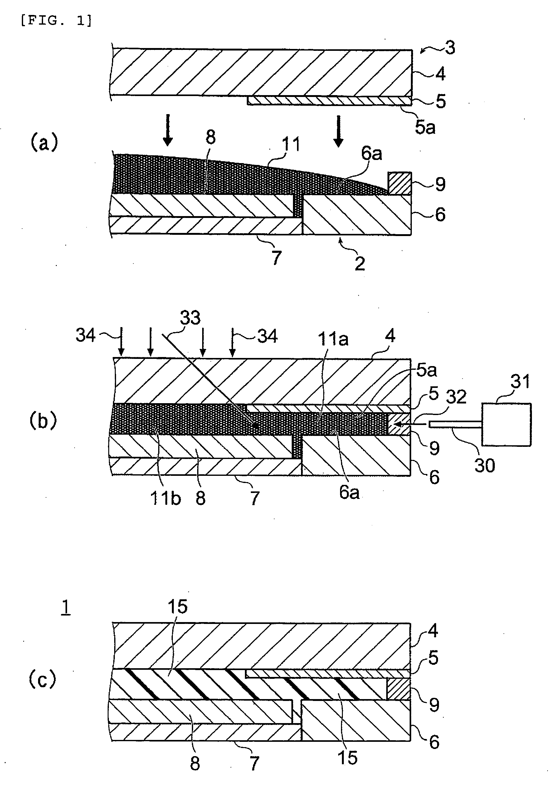
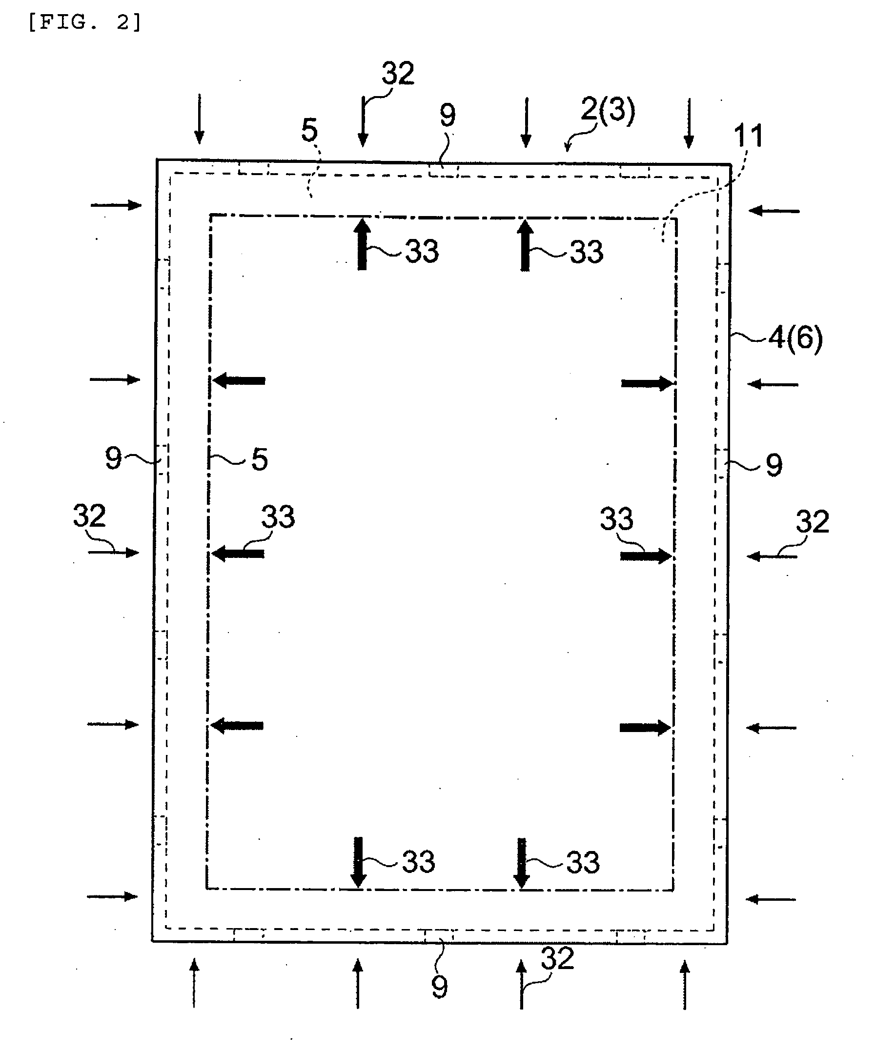
[0121]The resin compositions a and b (0.2 g each) were applied dropwise to the inner areas, surrounded by spacers, on liquid crystal display substrates as shown in FIG. 1(a), and acrylic plates each having a 2.0-mm wide light-shielding member and serving as a protection member were placed on the spacers. The resin compositions were photo-cured under conditions A to D described below, whereby liquid crystal display devices were produced as shown in Table 1.

[0122]The acrylic plates were removed from the obtained liquid crystal display devices, and the cure ratios of the cured products of the resin compositions a and b were measured in the manner described later. The results are shown in Table 1.

Curing Conditions A:

[0123]The resin composition was irradiated with UV rays at an integrated light quantity of 5,000 mJ using a UV lamp (product of USHIO Inc.) placed at a position about 10 cm away from the acrylic plate to be photo-cured, whereby a liquid crysta...

experimental example 1-2

[0128]The same procedure as in Experimental Example 1-1 was repeated except that an acrylic plate having a 5.0 mm-wide light-shielding member was used as the protection member. Liquid crystal display devices were produced using the resin compositions a and b under different curing conditions, and the cure ratio of the cured resin in each of the obtained liquid crystal devices was measured. The results are shown in Table 2.

TABLE 1Experimental Example 1-1 (Light-shielding member: 2 mm)Cure ratio of resin compositionLiquid crystalDirectly belowdisplay deviceCuringCentral portion oflight-shielding(resin composition)conditionsdisplay unitmember (2 mm)Resin composition aA95%50%B95%95%C95%95%D95%95%Resin composition bA95%50%C95%95%

Curing conditions A: Only the irradiation with UV rays from the acrylic plate side.

Curing conditions B: The irradiation with UV rays from the acrylic plate side and heating using a heater.

Curing conditions C: The irradiation with UV rays from the acrylic plate si...

experimental example 2

Measurement of Various Properties Of Cured Resins

[0132]The resin compositions a to g were applied dropwise to white glass plates having a thickness of 100 μm so as to have a predetermined thickness. The glass plates were carried into a UV conveyer, whereby the cured products of the resins having a predetermined thickness were obtained. These were used as samples. Each of the samples was measured for “light transmittance,”“storage elastic modulus,”“curing shrinkage ratio,” and “surface roughness,” as follows.

[Light Transmittance]

[0133]The light transmittance in the visible range was measured for each sample (the thickness of the cured resin: 100 μm) using an ultraviolet and visible spectrophotometer (V-560, product of JASCO Corporation) and was found to be 90% or more for all the samples.

[Storage Elastic Modulus]

[0134]The storage elastic modulus (Pa, 25° C.) was measured for each sample at a measurement frequency of 1 Hz using a viscoelasticity measuring apparatus (DMS 6100, product ...


PUM

PropertyMeasurementUnit
Temperatureaaaaaaaaaa
Fractionaaaaaaaaaa
Fractionaaaaaaaaaa

Abstract

A method for manufacturing an image display device includes the step of forming a cured resin layer 15 by interposing a photo-curable resin composition between a base 2 including an image display unit such as a liquid crystal display panel 8 and a light-transmitting protection member 3 including a light-shielding member 5 and then photo-curing the photo-curable resin composition. In this method, a resin composition having a curing shrinkage ratio of 5% or less, yielding a cured product having a storage elastic modulus at 25° C. of 1.0×10⁷ Pa or less, and forming the cured resin layer having a light transmittance of 90% or more in the visible range is used as the photo-curable resin composition.

Description

TECHNICAL FIELD[0001]The present invention relates to a method for manufacturing an image display device such as a liquid crystal display (LCD) device used, for example, in a cellular phone, and in particular, to a method for manufacturing an image display device having a transparent protection member disposed on the image display unit.BACKGROUND TECHNOLOGY[0002]One conventional example of such an image display device is a liquid crystal display device 101 shown in FIG. 7. This liquid crystal display device 101 includes a transparent protection member 103 made of, for example, glass or plastic and disposed on a liquid crystal display panel 102.[0003]In this case, to protect the surface of the liquid crystal display panel 102 and a polarizing plate (not shown), a spacer 104 is interposed between the liquid crystal display panel 102 and the protection member 103, so that a gap 105 is provided between the liquid crystal display panel 102 and the protection member 103.[0004]However, the...

Claims


Application Information

Patent Timeline
IPC IPC(8): C09K19/00B32B37/00
CPCG02F1/133308G02F1/1335G02F2001/133331Y10T428/1059G02F2202/023G02F2202/025G02F2202/28G02F2201/50G02F1/1333C09K2323/05G02F1/133331G02F1/1339
Inventor KAMATA, YUSUKESHINYA, YOSHIHISA
Owner DEXERIALS CORP
Why Eureka
Try Eureka