Compositions and methods for creating electronic circuitry

a technology of electronic circuits and compositions, applied in the field of manufacturing of conductive pathway patterns, can solve the problems of traces or paths that are not clean, circuit patterns (i.e. wiring configuration) are produced by a photolithography process that tends to be rather complex and costly, and the traces are generated from ablation

Inactive Publication Date: 2010-01-14
EI DU PONT DE NEMOURS & CO
View PDF101 Cites 13 Cited by
  • Summary
  • Abstract
  • Description
  • Claims
  • Application Information

AI Technical Summary

Benefits of technology

[0005]The present invention is directed to a printed circuit board precursor having an insulating substrate and a cover layer. The insulating

Problems solved by technology

Typically, the circuit pattern (i.e. wiring configuration) is produced by a photolithography process that tends to be rather complex and costly.
During the process of laser patternin

Method used


Image

  • Compositions and methods for creating electronic circuitry
  • Compositions and methods for creating electronic circuitry
  • Compositions and methods for creating electronic circuitry

Examples


Embodiment Construction

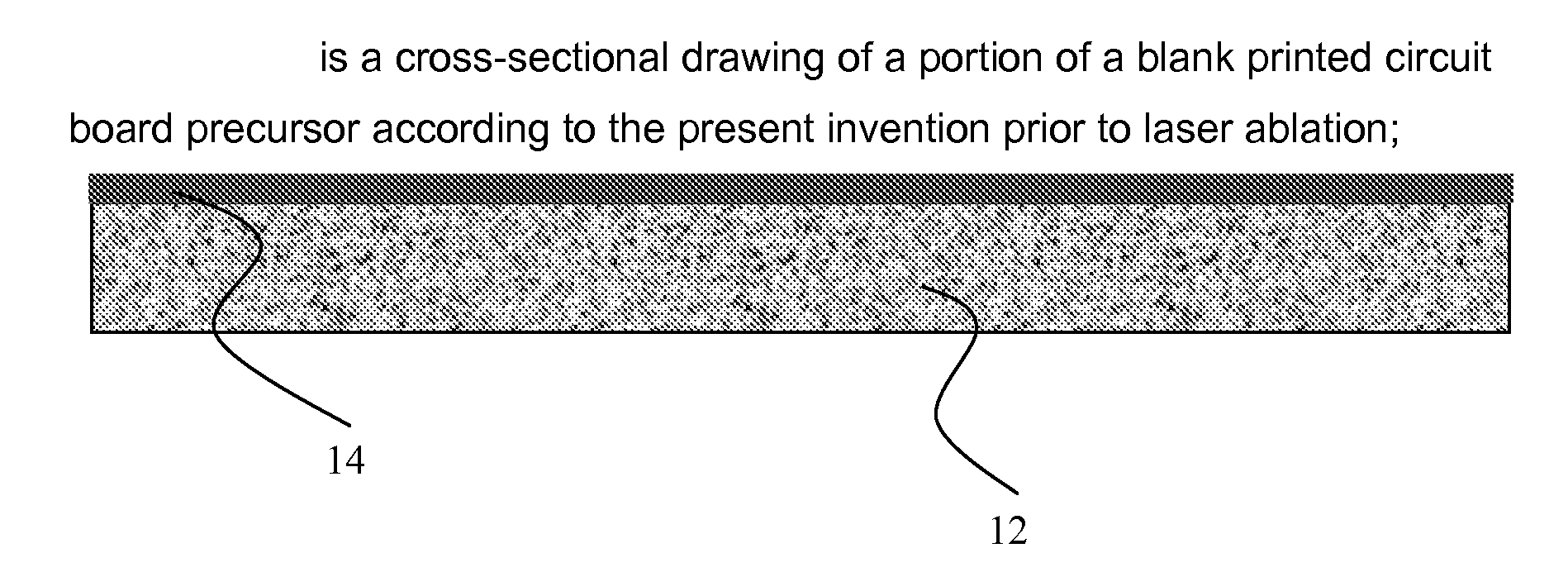
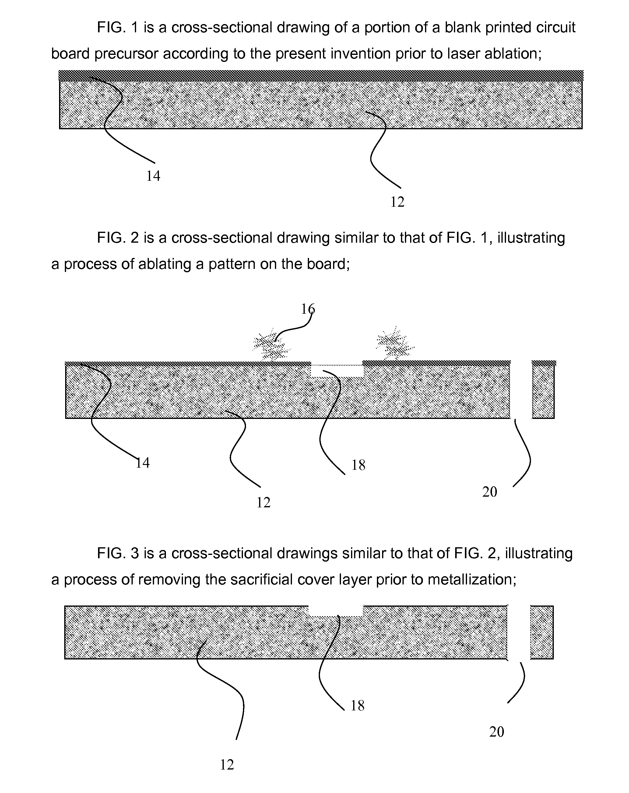
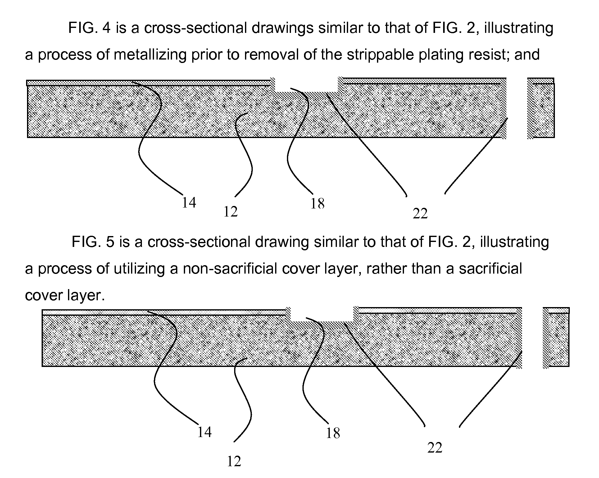
[0029]The present invention is directed to cover layers compositions for producing clean circuitry features. Referring now to the drawings, FIG. 1 illustrates one embodiment of the present invention, a printed circuit board (“PCB”) precursor 10. The PCB comprises a cover layer 14 and an insulating substrate 12 comprising an insulating matrix material and an activatable filler. A cover layer 14 is located over the insulating substrate.

[0030]Insulating substrate 12 comprises activatable filler interspersed within the insulating matrix material. In one embodiment, filler comprises two or more metal oxide cluster configurations within a definable crystal formation. The overall crystal formation, when in an ideal (i.e., non-contaminated, non-derivative) state, has the following general formula:

AB2O4

[0031]Where:[0032]i. A is a metal cation having a valance of 2, selected from a group including cadmium, chromium, manganese, nickel, zinc, copper, cobalt, iron, magnesium, tin, titanium, and...


PUM

PropertyMeasurementUnit
Percent by massaaaaaaaaaa
Thicknessaaaaaaaaaa

Abstract

The present invention is directed to non-lithographic patterning by laser (or similar-type energy beam) ablation, where the ablation system ultimately results in circuitry features that are relative free from debris induced over-plating defects (debris relating to the ablation process) and fully additive plating induced over-plating defects. Compositions of the invention include a circuit board precursor having an insulating substrate and a cover layer. The insulating substrate is made from a dielectric material and also a metal oxide activatable filler. The cover layer can be sacrificial or non-sacrificial and is used to remediate unwanted debris arising from the ablation process.

Description

FIELD OF THE INVENTION[0001]The present invention relates generally to the manufacture of conductive pathway patterns for printed circuit materials. More particularly, the processes and materials of the present invention are directed to non-lithographic patterning by laser or similar-type energy beam ablation, where the ablation system ultimately results in circuitry features that are relatively free from debris induced over-plating defects (debris relating to the ablation process) and fully additive plating induced over-plating defects.BACKGROUND OF THE INVENTION[0002]Printed circuit boards (PCBs) typically comprise an insulating substrate (e.g., glass fiber reinforced epoxy or polyimide film) which supports a thin conducting layer (usually copper) in a pattern designed for a specific application. The patterned conducting layer (also referred to as a printed circuit), is the means for carrying electrical voltages and currents between various electrical components, such as resistors...

Claims


Application Information

Patent Timeline
IPC IPC(8): B32B27/08H05K3/00B05D3/10C08J7/18
CPCB32B27/08B32B27/18B32B27/20H05K1/0373H05K3/0032Y10T428/26H05K3/185H05K2201/0112H05K2201/0236H05K2203/107Y10T29/49156H05K3/184B32B5/147B32B27/281B32B27/302B32B27/308B32B27/322B32B27/34B32B27/36B32B27/38B32B2260/021B32B2260/046B32B2262/101B32B2264/102B32B2270/00B32B2307/206B32B2307/714B32B2457/00Y10T428/31504Y10T428/31511Y10T428/3154Y10T428/31721Y10T428/31725Y10T428/31786Y10T428/31855Y10T428/31942
Inventor LEE, YUEH-LINGFANG, SHANE
Owner EI DU PONT DE NEMOURS & CO
Why Eureka
Try Eureka