Substrate structure and method of removing the substrate structure

a substrate structure and substrate technology, applied in the field of substrate structure removal, can solve the problems of low yield rate of this method, low efficiency of the above-mentioned process, non-uniformity problem, etc., and achieve the effect of reducing process cost, increasing reaction area for etching, and increasing efficiency of etching process to separate semiconductor layers from substrates

Inactive Publication Date: 2010-01-14
ADVANCED OPTOELECTRONICS TECH
View PDF11 Cites 17 Cited by
  • Summary
  • Abstract
  • Description
  • Claims
  • Application Information

AI Technical Summary

Benefits of technology

[0013]This invention utilizes spaces between a plurality of pillars to substantially increase reaction areas for etching. Therefore, by using the method of the invention the efficiency of an etching process to separate a semiconductor layer from a substrate can be increased and the cost for a process can be reduced.

Problems solved by technology

The efficiency of the above-mentioned process is low.
In addition, removal of the substrate with only the wet etching process incurs a non-uniformity problem.
However, the yield rate of this method is low and the LiAlO2 substrate is too fragile to use this method.
Accordingly, this method also incurs low efficiency of removing substrates and non-uniformity problems.
These methods all lead to problems of low removal efficiency, non-uniformity, or fragility.
Such devices for separating are expensive.
In addition, warpage problems are caused due to thicker epitaxy layers.
Such devices for separating are expensive.
In addition, warpage problems are caused due to thicker epitaxy layers.

Method used


Image

  • Substrate structure and method of removing the substrate structure
  • Substrate structure and method of removing the substrate structure
  • Substrate structure and method of removing the substrate structure

Examples


Embodiment Construction

[0021]A semiconductor process is described in accordance with the present invention. Detailed structural elements are described as follows to realize this invention thoroughly. The embodiments of the present invention do not limit the details that are familiar to persons skilled in the light source module fields. On the other hand, well known elements are not described in detail to prevent the introduction of unnecessary limitations. Preferred embodiments are described in detail as follows. In addition to these detailed descriptions, this invention can also be implemented in a wide range of other embodiments. Furthermore, the scope of the present invention is not to be taken in a limiting sense, and is defined only by the appended claims.

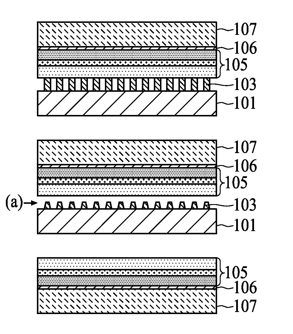
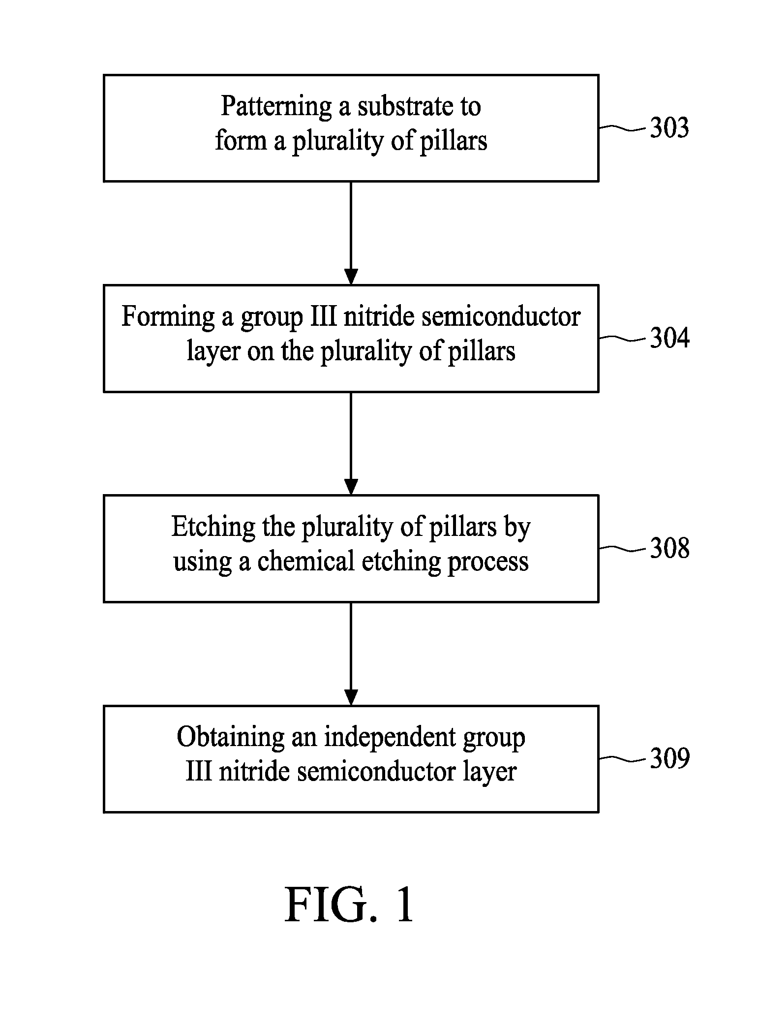
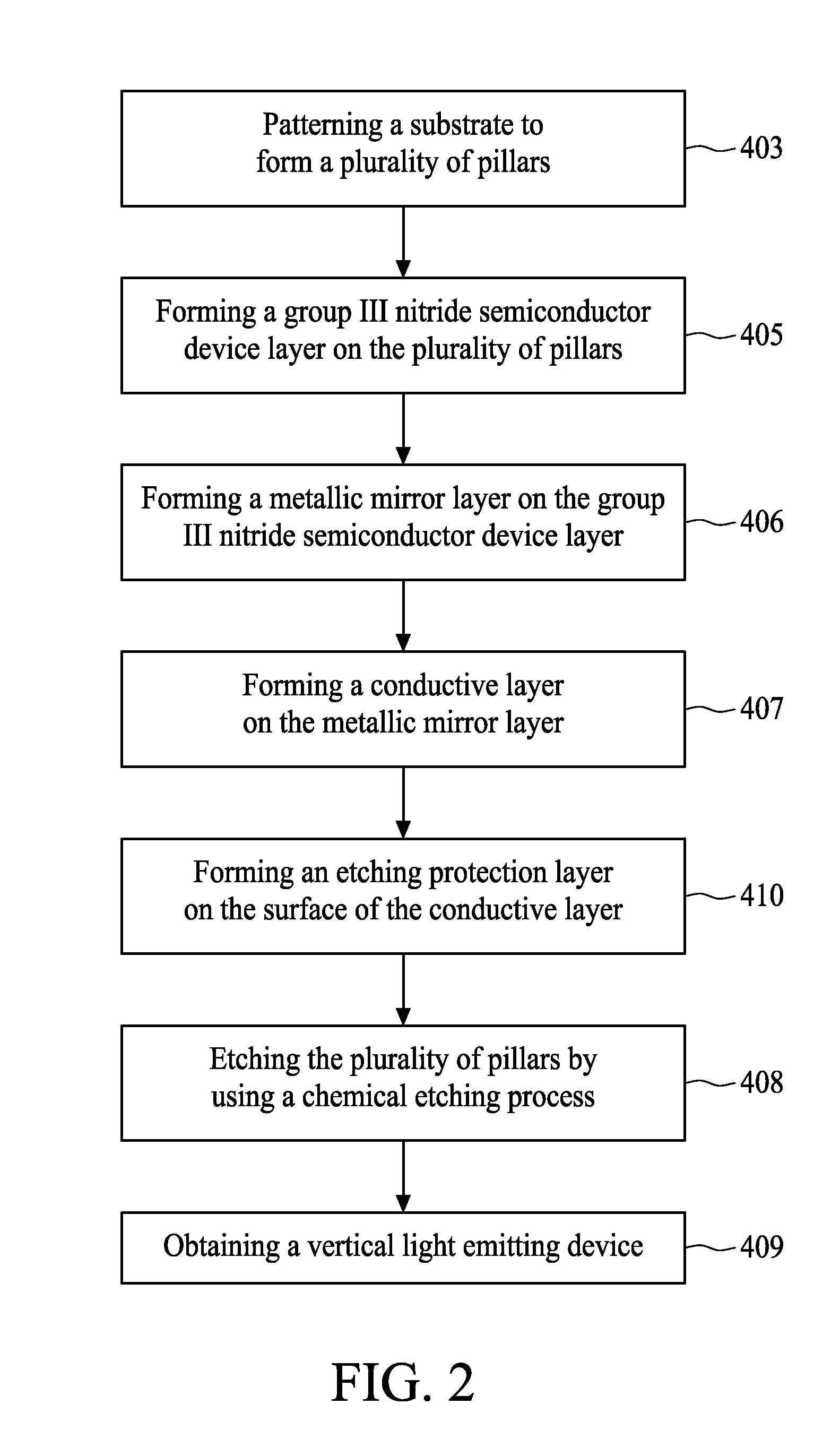
[0022]FIG. 1 illustrates a flowchart of a method for removing a substrate structure in accordance with the first preferred embodiment of the present invention. FIG. 3A and FIG. 3B illustrate the diagram of each cross-sectional structure during the p...


PUM


Abstract

A method of removing a substrate structure is described. A plurality of pillars is formed on a substrate by using a photolithography etching process. A group III nitride semiconductor layer is grown on the plurality of pillars. The plurality of pillars is etched to separate the group III nitride semiconductor layer from the substrate by using a chemical etching process.

Description

BACKGROUND OF THE INVENTION[0001]1. Field of the Invention[0002]The present invention relates to a semiconductor process, and more particularly, to a method for removing a substrate structure.[0003]2. Description of the Related Art[0004]Several prior arts disclose how to remove a substrate. For example, U.S. Pat. No. 6,648,966 and U.S. Pat. No. 7,169,227 respectively disclose methods for making a GaN wafer, wherein a material of the substrate is LiAlO2. The thickness of the substrate is about 430 μm. The substrate is completely removed by using a wet etching process for several days (the acid etching rate for LiAlO2 is about 15-30 nm / minute at room temperature). The efficiency of the above-mentioned process is low. In addition, removal of the substrate with only the wet etching process incurs a non-uniformity problem.[0005]Moreover, U.S. Pat. No. 6,218,280 discloses that a LiAlO2 substrate is peeled off by the application of mechanical force. However, the yield rate of this method i...

Claims


Application Information

Patent Timeline
Patent Type & Authority Applications(United States)
IPC IPC(8): H01L33/00H01L21/205
CPCH01L21/0254H01L33/0079H01L21/02653H01L21/02639H01L33/0093
Inventor TU, PO MINHUANG, SHIH CHENGCHAN, SHIH HSIUNG
Owner ADVANCED OPTOELECTRONICS TECH
Why Eureka
Try Eureka