Printed circuit board design support program, recording medium, and printed circuit board design support method

a printed circuit board and support method technology, applied in the direction of cad circuit design, cross-talk/noise/interference reduction, instruments, etc., can solve the problem of taking a long time for users to determin

Active Publication Date: 2010-01-14
CANON KK
View PDF1 Cites 11 Cited by
  • Summary
  • Abstract
  • Description
  • Claims
  • Application Information

AI Technical Summary

Problems solved by technology

In recent years, in association with an increase in the speed of signals transmitted in an electronic device such as an information technology device, unnecessary electromagnetic waves (hereinafter, referred to as radiation noise) radiated from the electronic device cause a problem.
Therefore, it takes much time for the user to determine the location at which the via can be additionally arranged, and further, a mistake in the determination or an oversight of the position where the additional arrangement can be performed may occur.

Method used


Image

  • Printed circuit board design support program, recording medium, and printed circuit board design support method
  • Printed circuit board design support program, recording medium, and printed circuit board design support method
  • Printed circuit board design support program, recording medium, and printed circuit board design support method

Examples


first embodiment

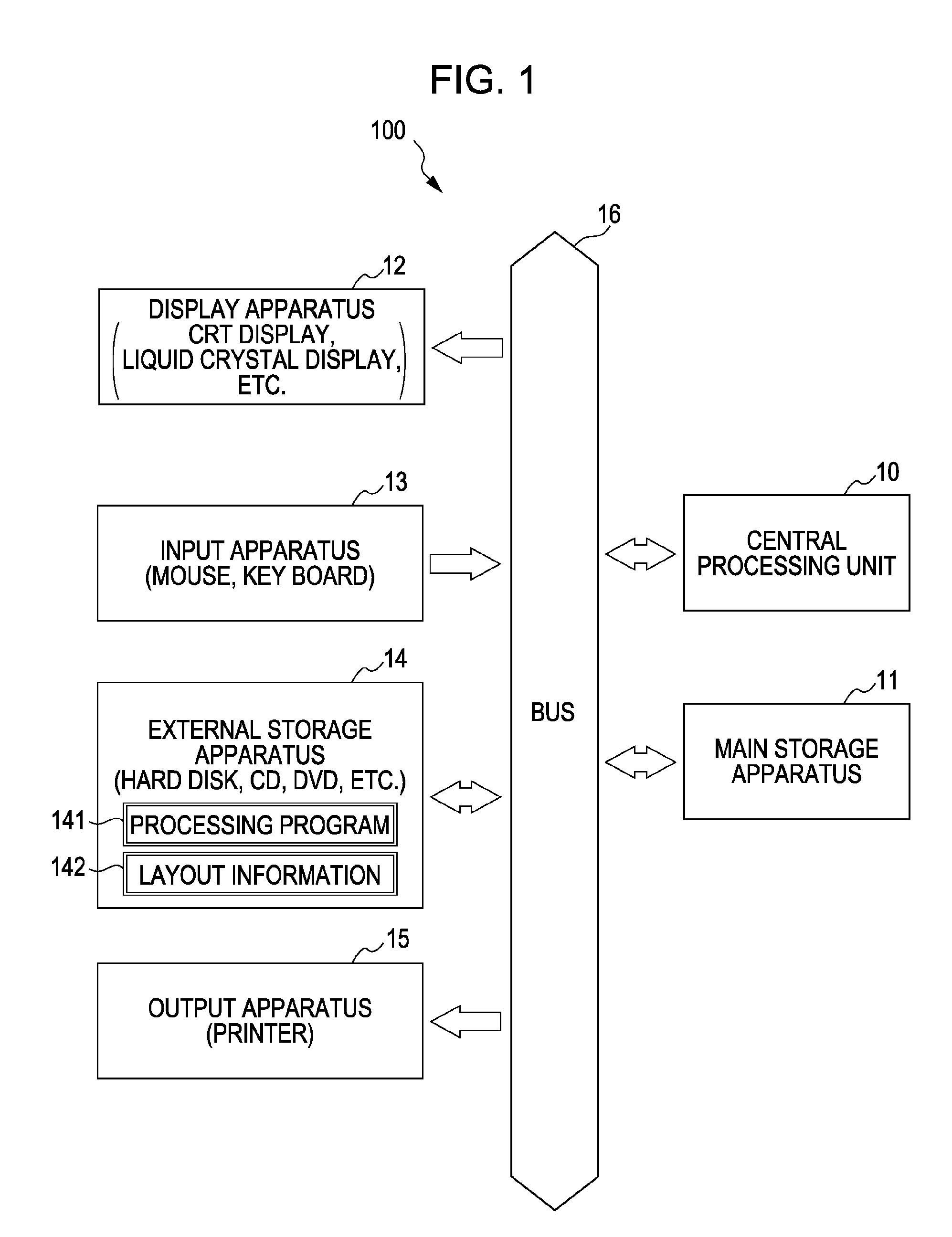
[0079]FIG. 1 shows an example of a schematic configuration of a computer apparatus including a printed circuit board design support apparatus according to the present invention. As shown in FIG. 1, a printed circuit board design support apparatus 100 is constructed by including a central processing unit (CPU) 10, a main storage apparatus 11, a display apparatus 12, an input apparatus 13, an external storage apparatus 14, and an output apparatus 15.

[0080]The CPU 10 is configured to control the entirety of the apparatus. The main storage apparatus 11 is composed of a read-only store memory (ROM), a random access memory (RAM) for temporarily performing read and write when the CPU 10 performs a calculation processing, or the like. The display apparatus 12 is composed of a cathode-ray tube, a liquid crystal display, or the like. The input apparatus 13 is composed of a mouse, a key board, or the like. The external storage apparatus 14 is configured to perform read and write with respect t...

third embodiment

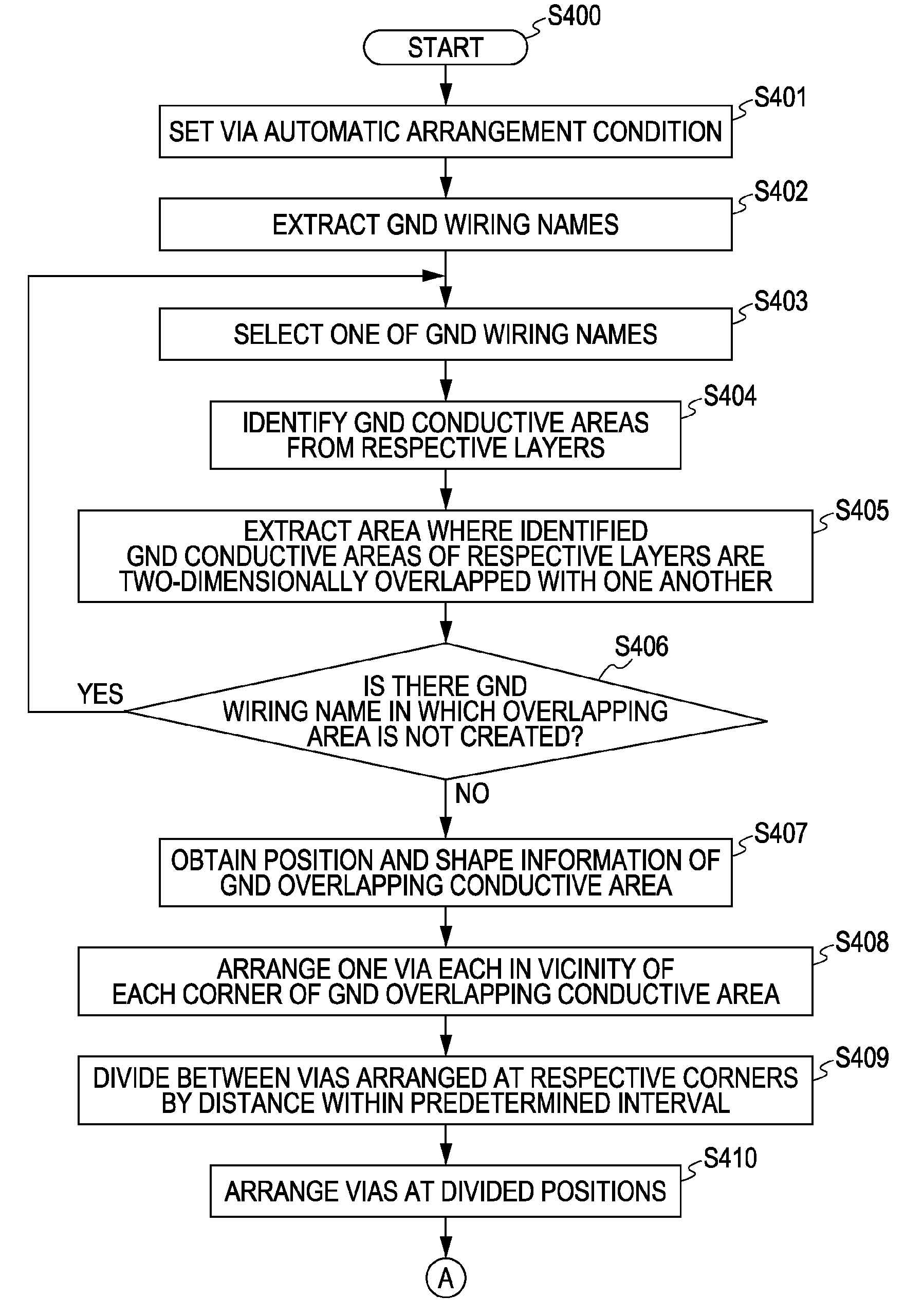
[0289]In addition, according to the present embodiment, the case has been described in which the GND overlapping conductive area is divided into the peripheral edge part and the inner edge part, and the central part, and the GND vias are rearranged in a stepwise fashion, but by the GND via arrangement method the GND via can be rearranged without the division in a stepwise fashion.

[0290]According to the present embodiment, similarly as in the first embodiment, by allowing the user to set the shift distance in step S412 and the search range for the surrounding of the slide position in step S414, it is possible to realize the arrangement state of the GND vias desired by the user. With this setting, by decreasing the number of the GND vias to be arranged instead of arranging the GND vias within the predetermined interval, it is possible to carry out the arrangement of the GND vias in consideration of cost aspects. Furthermore, even in a case where the position information and the shape...

fifth embodiment

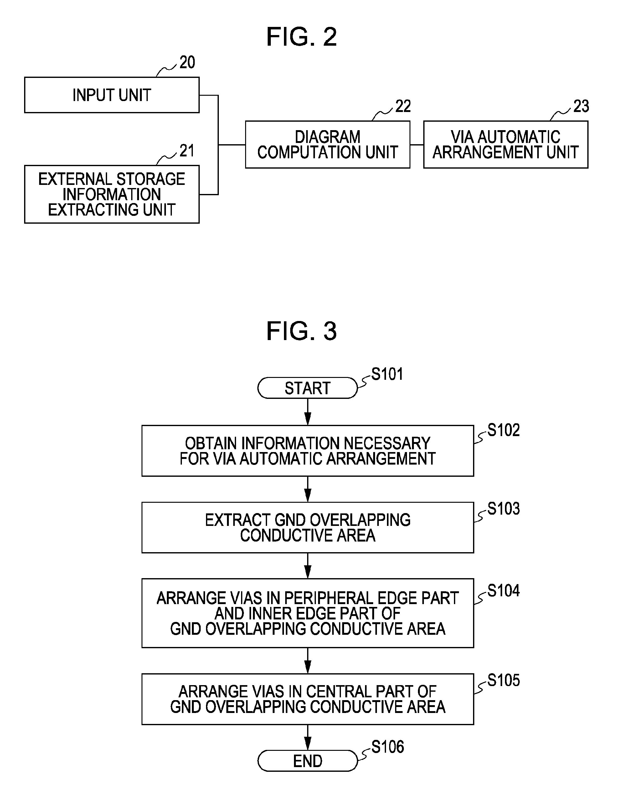
[0295]First, the flow chart shown in FIG. 45 will be described in detail. Herein, the flow chart shown in FIG. 45 is obtained by adding steps S4300, S4301 and S4302 after the start of the flow chart in FIG. 35 shown. Therefore, only details of steps S4300, S4301 and S4302 will be described.

[0296]In step S4300, the external storage information extracting unit 21 obtains via arrangement prohibition area information with respect to the respective components and wirings arranged on the printed circuit board. This processing corresponds to a prohibition area information obtaining step. For a method of obtaining the via arrangement prohibition area information, it is preferably to use a method in which the via arrangement prohibition area information is included in the layout information 142, and the external storage information extracting unit 21 obtains via arrangement prohibition area information from the layout information 142 stored in the main storage apparatus 11. It is to be note...


PUM


Abstract

To automatically arrange vias on a printed circuit board so as to satisfy a predetermined condition. A printed circuit board design support method for causing a computer to execute a ground conductive area identifying conductive areas which can be used as grounds of a printed circuit board having a plurality of condicutive layers, an extracting an overlapping conductive area in which the conductive areas identified in the ground conductive area identifying are two-dimensionally overlapped with one another, and an automatic arranging interlayer connection members configured to electrically connect at least two layers with one another among the plurality of conductive areas in the overlapping conductive area extracted in the extracting at an interval within a predetermined distance.

Description

BACKGROUND OF THE INVENTION[0001]1. Field of the Invention[0002]The present invention relates to a printed circuit board design support program, a recording medium, a printed circuit board design support method, and a printed circuit board design support apparatus. In particular, the invention aims to appropriately arrange an interlayer connection member (a via hole, hereinafter, referred to as “via”) configured to electrically connect a plurality of conductive layers laminated on contact with an insulating layer.[0003]2. Description of the Related Art[0004]In recent years, in association with an increase in the speed of signals transmitted in an electronic device such as an information technology device, unnecessary electromagnetic waves (hereinafter, referred to as radiation noise) radiated from the electronic device cause a problem. In order to solve this problem, various designs for suppressing the radiation noise are carried out with respect to a wiring on a printed circuit boa...

Claims


Application Information

Patent Timeline
Patent Type & Authority Applications(United States)
IPC IPC(8): G06F17/50
CPCG06F17/5068H05K1/0218H05K2201/09618H05K2201/093H05K2201/09309H05K3/0005G06F30/39
Inventor SADAMATSU, TOSHISATO
Owner CANON KK
Why Eureka
Try Eureka