

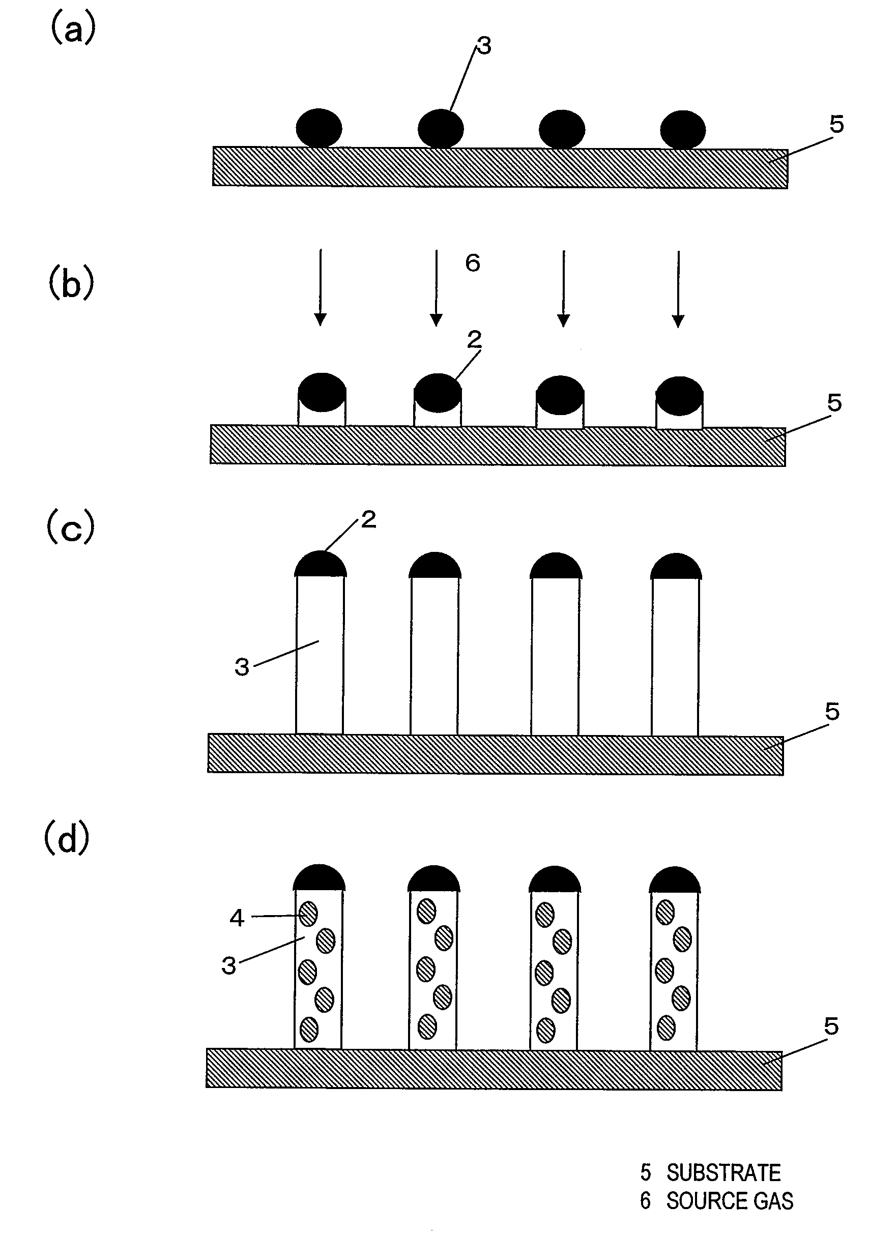
Nanowire, device comprising nanowire, and their production methods
a nanowire and nanotechnology, applied in the direction of nanoinformatics, crystal growth process, polycrystalline material growth, etc., can solve the problems of limited miniaturization by a conventional lithography technique, rapid increase of the cost of the exposure apparatus and the mask member, etc., to eliminate the complexity of the production process and the poor reproducibility and productivity. , the effect of easy control
- Summary
- Abstract
- Description
- Claims
- Application Information
AI Technical Summary
Benefits of technology
Problems solved by technology
Method used
Image

Examples
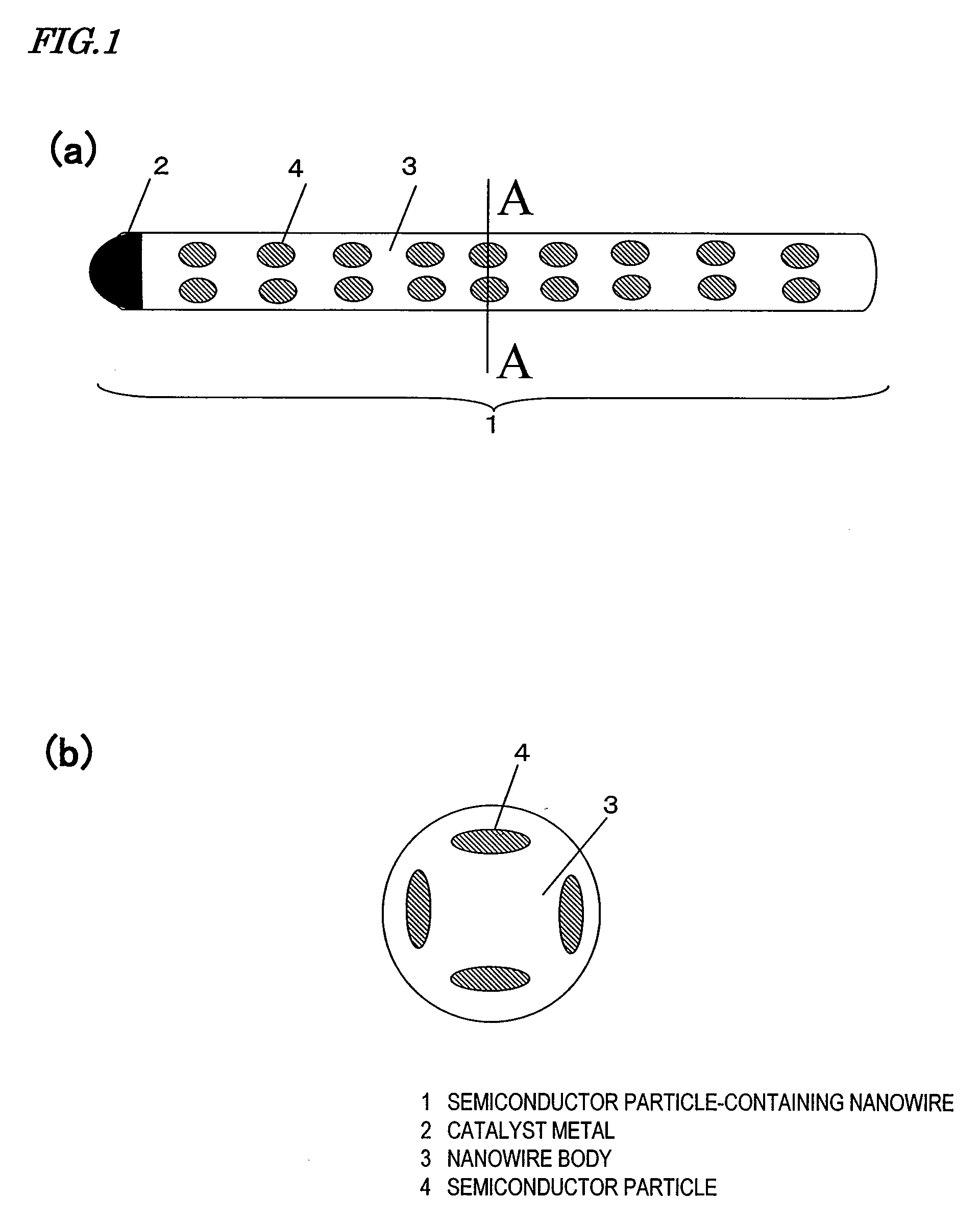
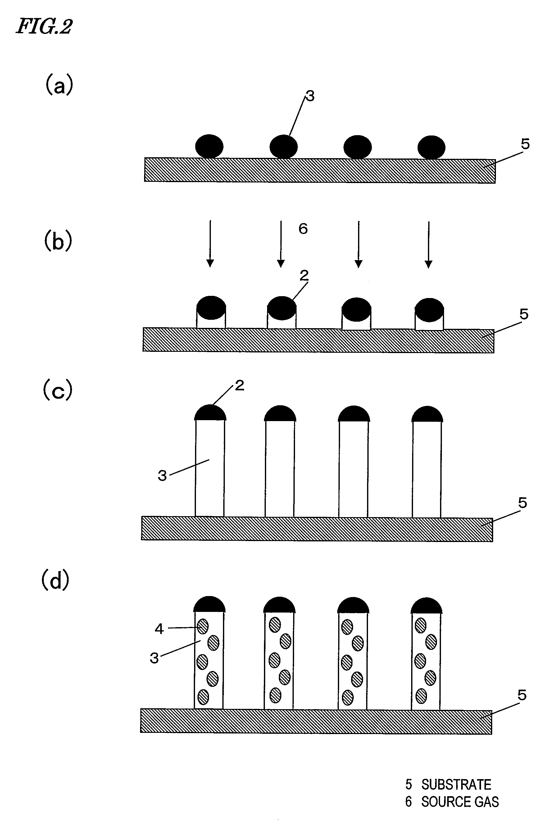
embodiment 1
[0111]First, with reference to FIG. 3 to FIG. 5, a first embodiment of the nanowire according to the present invention will be described. The nanowire of the present embodiment is a nanowire such that germanium (Ge) particles are contained in a silicon germanium nanowire (SiGe) body, and hereinafter will be referred to as a “Ge particle-containing SiGe nanowire”.
[0112]FIG. 3 is a photograph showing an example of a transmission electron microscope (TEM) image of the Ge particle-containing SiGe nanowire 110 according to the present embodiment. FIG. 4 is a photograph showing an enlarged TEM image of section X in FIG. 3. FIG. 5(a) is a graph showing an element analysis result of the region of point 2 in FIG. 4, whereas FIG. 5(b) is a graph showing an element analysis result of the region of point 1 in FIG. 4.
[0113]The Ge particle-containing SiGe nanowire 110 shown in FIG. 3 is structured so that a plurality of Ge particles 112 are located in the interior of a SiGe nanowire body 111. In ...
embodiment 2
[0147]Next, with reference to FIG. 7, an embodiment of a nanowire light-emission device according to the present invention will be described. This light-emission device includes a light-emitting region which is made of semiconductor particle-containing nanowires. A nanowire of the present embodiment has a hetero structure such that a semiconductor particle-containing nanowire and nanowires for contact purposes which do not contain any semiconductor particles are jointed. Hereinafter, such a nanowire will be referred to as a “hetero nanowire”.
[0148]FIG. 7(a) is a cross-sectional view showing the structure of a hetero nanowire 202 in the present embodiment, whereas FIG. 7(b) is a perspective view showing a nanowire light-emission device 201 in which the hetero nanowires 202 are used. Hereinafter, the structure of the nanowire light-emission device 201 will be described.
[0149]In the hetero nanowire 202 shown in FIG. 7(a), nanowires 206 for contact purposes are connected to both ends of...
embodiment 3
[0170]Next, with reference to FIG. 10 and FIG. 11, a third embodiment of the nanowire according to the present invention will be described. In the nanowire of the present embodiment, a plurality of hetero structures are present within one nanowire, each hetero structure being constituted by a Ge particle-containing nanowire described in Embodiment 1 and a nanowire not containing any Ge particles. Such a nanowire will be referred to as a “multi Ge particle-containing nanowire”.
[0171]FIG. 10 is a cross-sectional view showing the structure of a multi Ge particle-containing nanowire 301 according to the present embodiment. FIG. 11 is a diagram showing a production method for the nanowire of the present embodiment.
[0172]The multi Ge particle-containing nanowire 301 shown in FIG. 10 includes a plurality of regions 303 where Ge particles exist and regions 302 where Ge particles are absent. A feature of the present embodiment is that the regions 303 where Ge particles exist are composed of ...
PUM
| Property | Measurement | Unit |
|---|---|---|
| wavelength | aaaaa | aaaaa |
| diameter | aaaaa | aaaaa |
| diameter | aaaaa | aaaaa |
Abstract
Description
Claims
Application Information