Solder Interconnect

a technology of interconnects and solid-state devices, applied in the direction of semiconductor devices, semiconductor/solid-state device details, electrical devices, etc., can solve the problems of grain coarsening, adversely affecting product reliability, and fatigue stress due to thermal expansion mismatch, and achieve the effect of shrinking grain sizes

Inactive Publication Date: 2010-01-21
GLOBALFOUNDRIES INC
View PDF10 Cites 5 Cited by
  • Summary
  • Abstract
  • Description
  • Claims
  • Application Information

AI Technical Summary

Benefits of technology

[0009]In accordance with one aspect of the present invention, a method of manufacturing is provided that includes coupling a semiconductor chip to a circuit board with plural solder joints whereby an interstitial space is left between the semiconductor chip and the circuit board. The semiconductor chip and the circuit board are heated at a first temperature lower than a melting point of constitu

Problems solved by technology

Consequently, fatigue stresses due to thermal expansion mismatch is of great concern.
Any voids remaining in the underfill after solidification can adversely impact product reliability.
The pre-bake, though necessary, introduces another issue: grain coarsening.
Conventional f

Method used


Image

  • Solder Interconnect
  • Solder Interconnect
  • Solder Interconnect

Examples


Embodiment Construction

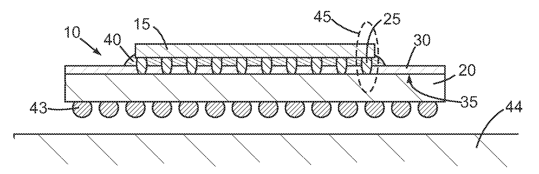
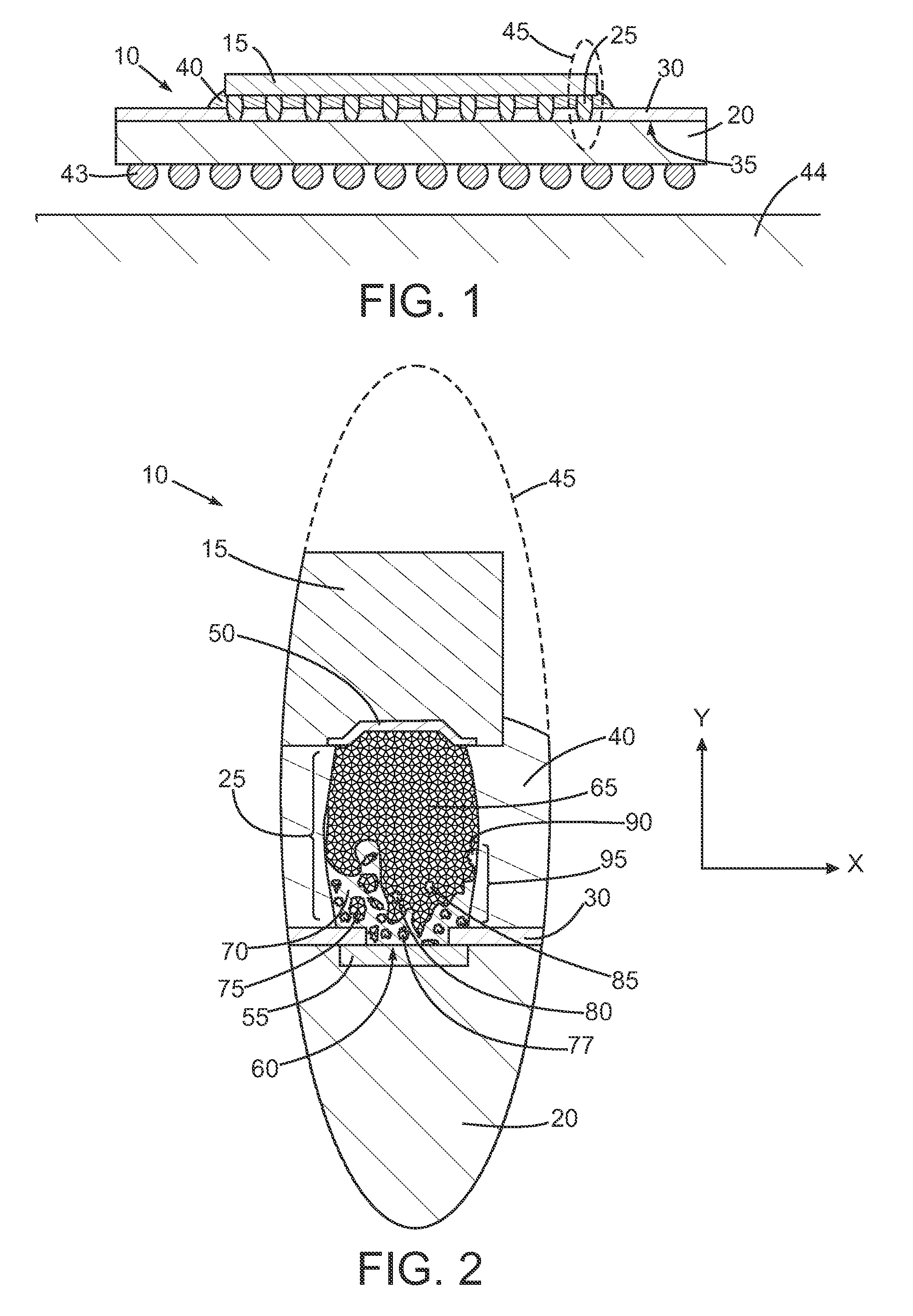
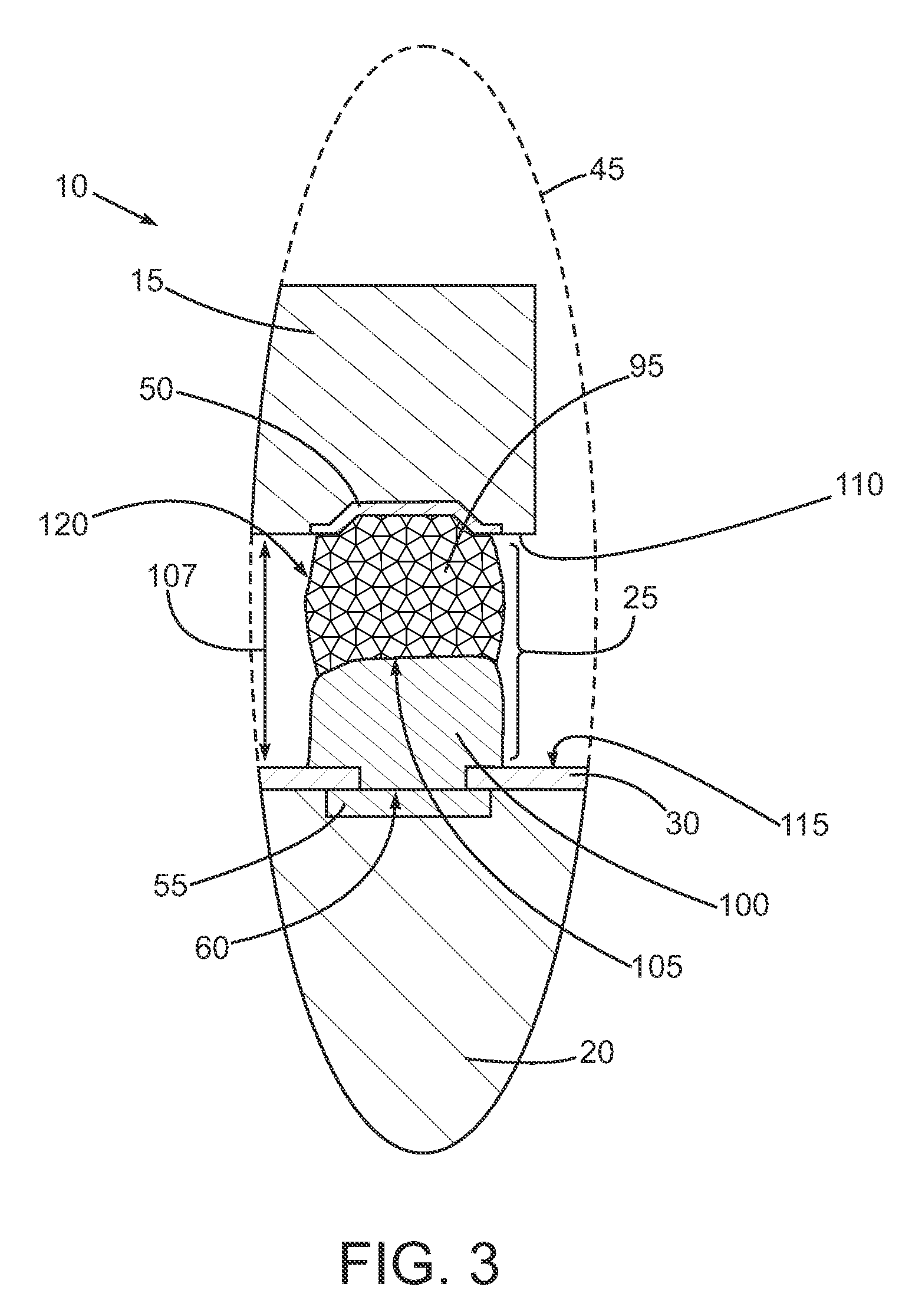
[0020]In the drawings described below, reference numerals are generally repeated where identical elements appear in more than one figure. Turning now to the drawings, and in particular to FIG. 1, therein is shown a sectional view of an exemplary conventional semiconductor chip package 10 that includes a semiconductor chip 15 mounted in flip-chip fashion on a package substrate 20. Electrical interconnections between the chip 15 and the package substrate 20 are provided by way of a plurality of solder joints 25. A solder mask 30 is provided on the upper surface 35 of the substrate 20 in order to facilitate the fabrication of the solder joints 25. An underfill material layer 40 is positioned between the chip 15 and the solder mask 30. The underfill material layer 40 is designed to alleviate some of the stresses on the solder joints 25 as a result of substantial differences in the CTE of the chip 15 and the substrate 20. The package 10 may be lidless as depicted or optionally provided w...


PUM


Abstract

Various solder interconnect methods and apparatus are disclosed. In aspect, a method of manufacturing is provided that includes coupling a semiconductor chip to a circuit board with plural solder joints whereby an interstitial space is left between the semiconductor chip and the circuit board. The semiconductor chip and the circuit board are heated at a first temperature lower than a melting point of constituents of the plural solder joints to liberate contaminants from the interstitial space. The semiconductor chip and the circuit board are heated again at a second temperature higher than a melting point of at least one the constituents but not all of the constituents of the plural solder joints to shrink grain sizes of the at least one constituent. An underfill is placed in the interstitial space.

Description

BACKGROUND OF THE INVENTION[0001]1. Field of the Invention[0002]This invention relates generally to semiconductor processing, and more particularly to methods and apparatus for connecting a semiconductor chip to a circuit board.[0003]2. Description of the Related Art[0004]Conventional semiconductor chips are often mounted on and electrically connected to a printed circuit board of one sort or another. Examples include package substrates or chip carriers, motherboards, application specific cards and others. Surface mounting is one type of mounting / interconnect technique and there are several variants of this basic technique. One very widely-used technique is flip-chip controlled collapse chip connection (C4) in which electrical connections between the chip and the package substrate, board etc. are established by creating an array of C4 solder joints. In one type of conventional lead-based process, an array of high lead content tin-lead (97Pb 3Sn) solder bumps are formed on conducting...

Claims


Application Information

Patent Timeline
IPC IPC(8): H01L21/56
CPCH01L21/563H01L23/3128H01L24/16H01L24/92H01L2224/05572H01L2224/05639H01L2224/05644H01L2224/05647H01L2224/05664H01L2224/05669H01L2224/11849H01L2224/13116H01L2224/13139H01L2224/13144H01L2224/13147H01L2224/13169H01L2224/16502H01L2224/73204H01L2224/81047H01L2224/81193H01L2224/81211H01L2224/81411H01L2224/81805H01L2224/81815H01L2224/81948H01L2224/81986H01L2224/83048H01L2224/83102H01L2224/83104H01L2224/92125H01L2924/01029H01L2924/01046H01L2924/01078H01L2924/01079H01L2924/01082H01L2924/01322H01L2924/14H01L2924/15311H01L2924/01006H01L2924/01019H01L2924/01033H01L2924/01047H01L2924/10253H01L2224/0401H01L2924/0002H01L2924/00014H01L2924/0105H01L2224/83H01L2924/00H01L2224/05552
Inventor KHAN, MOHAMMADGANNAMANI, RANJITZHAI, CHARLIESENGUPTA, SHIRSHONEWMAN, ROBERT
Owner GLOBALFOUNDRIES INC
Why Eureka
Try Eureka