
Method and apparatus for surface treatment of semiconductor substrates using sequential chemical applications

a technology of semiconductor substrates and chemical applications, applied in the direction of cleaning processes and apparatus, cleaning using liquids, semiconductor/solid-state device testing/measurement, etc., can solve the problems of inefficient removal of polymer residues, material or chemical used in fabrication operations to which the substrate is exposed, and potential source of contamination, etc., to achieve the effect of efficiently removing polymer residue contaminants

Inactive Publication Date: 2010-01-28
LAM RES CORP
View PDF2 Cites 21 Cited by
  • Summary
  • Abstract
  • Description
  • Claims
  • Application Information

AI Technical Summary

Benefits of technology

[0008]The present invention fills the need by providing improved methods and apparatus for efficiently removing polymer residue contaminants formed around a metal gate structure on the surface of the substrate. It should be appreciated that the present invention can be implemented in numerous ways, including an apparatus and a method. Several inventive embodiments of the present invention are described below.
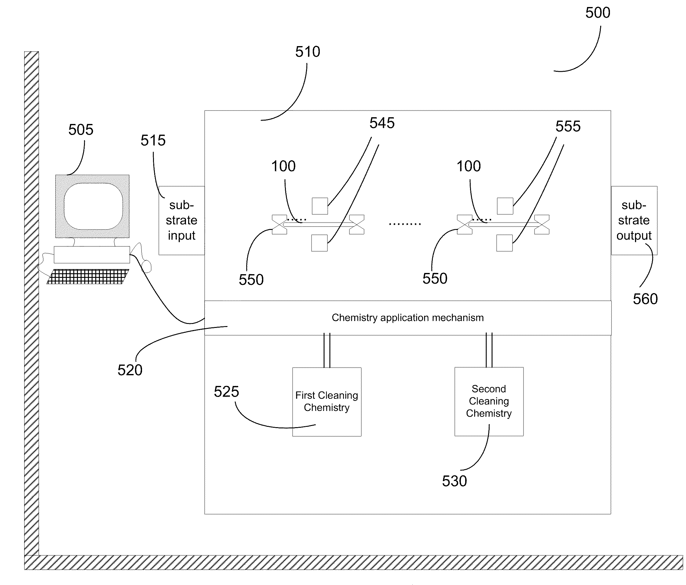
[0010]In another embodiment, a system for removing polymer residue from around a metal gate structure formed on a surface of a substrate during a post-etch cleaning operation, is defined. The system includes a substrate supporting device to receive, support and transport the substrate through the system. A first proximity head is configured to introduce a first cleaning chemistry to a portion of the surface of the substrate as a meniscus. A second proximity head is configured to introduce a second cleaning chemistry to the portion of the surface of the substrate as a meniscus. The introduction of the first and second cleaning chemistries sequentially through the first and second proximity heads enables application of the first and second cleaning chemistries in a controlled manner to the portion of the surface of the substrate so that the portion of the surface of the substrate is optimally exposed to the first and second cleaning chemistries for an optimal period of time for substantial removal of the polymer residue formed around the metal gate structure while the structural integrity of the one or more layers of the gate structure is maintained.

Problems solved by technology

Any material or chemical used in the fabrication operations to which the substrate is exposed is a potential source of contamination.
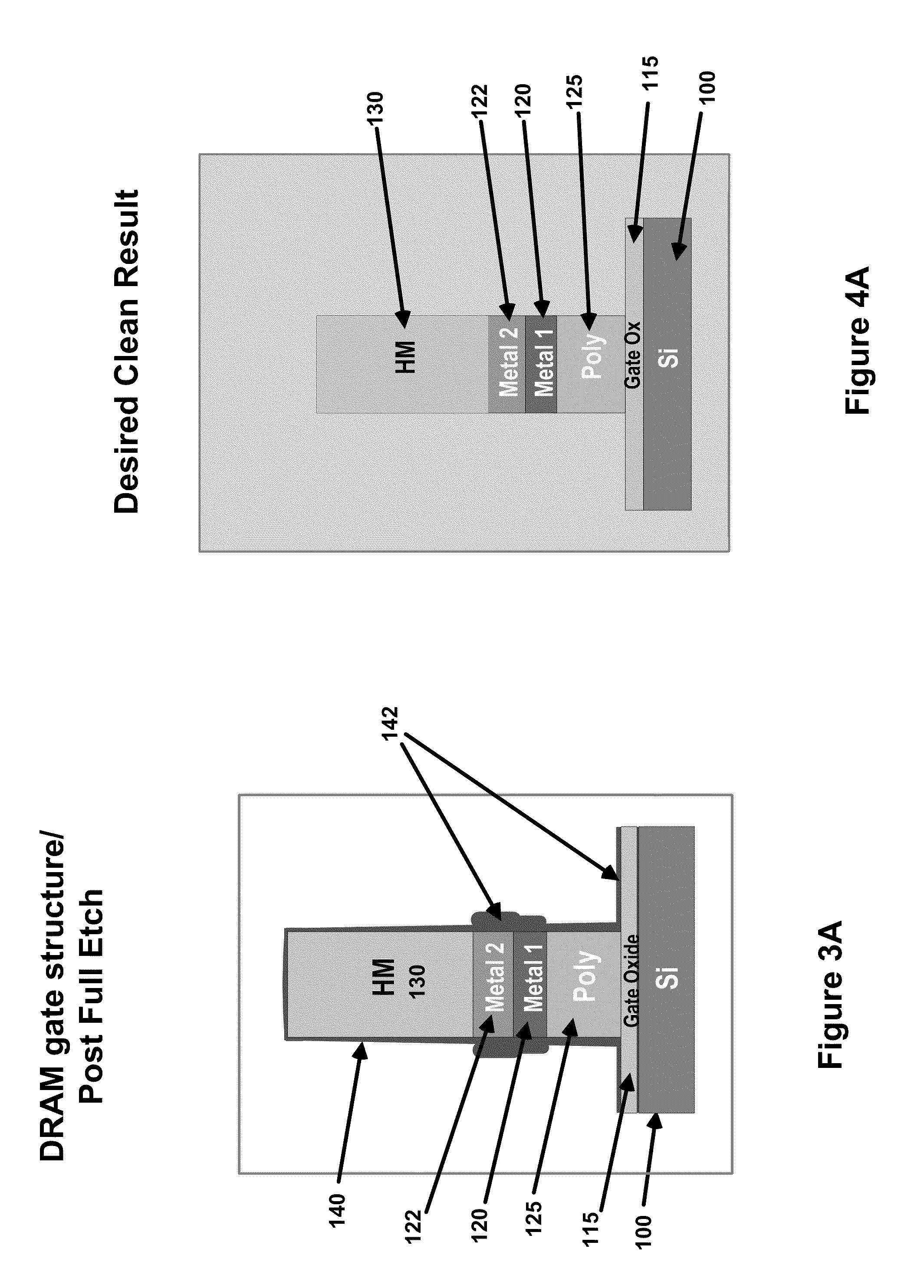
These contaminants lodge on the top, along the side walls and in between the features in hard-to-reach areas, such as in a trench surrounding the delicate features, and may likely cause damage to the features within the vicinity of the contaminant particles.
When a less aggressive cleaning chemistry is used, the exposure results in inefficient removal of polymer residues and other contaminants.
On the other hand, when a more aggressive chemistry is used, the exposure using the batch tools leads to high material loss rates at the gate structure rendering the cleaning process undesirable.
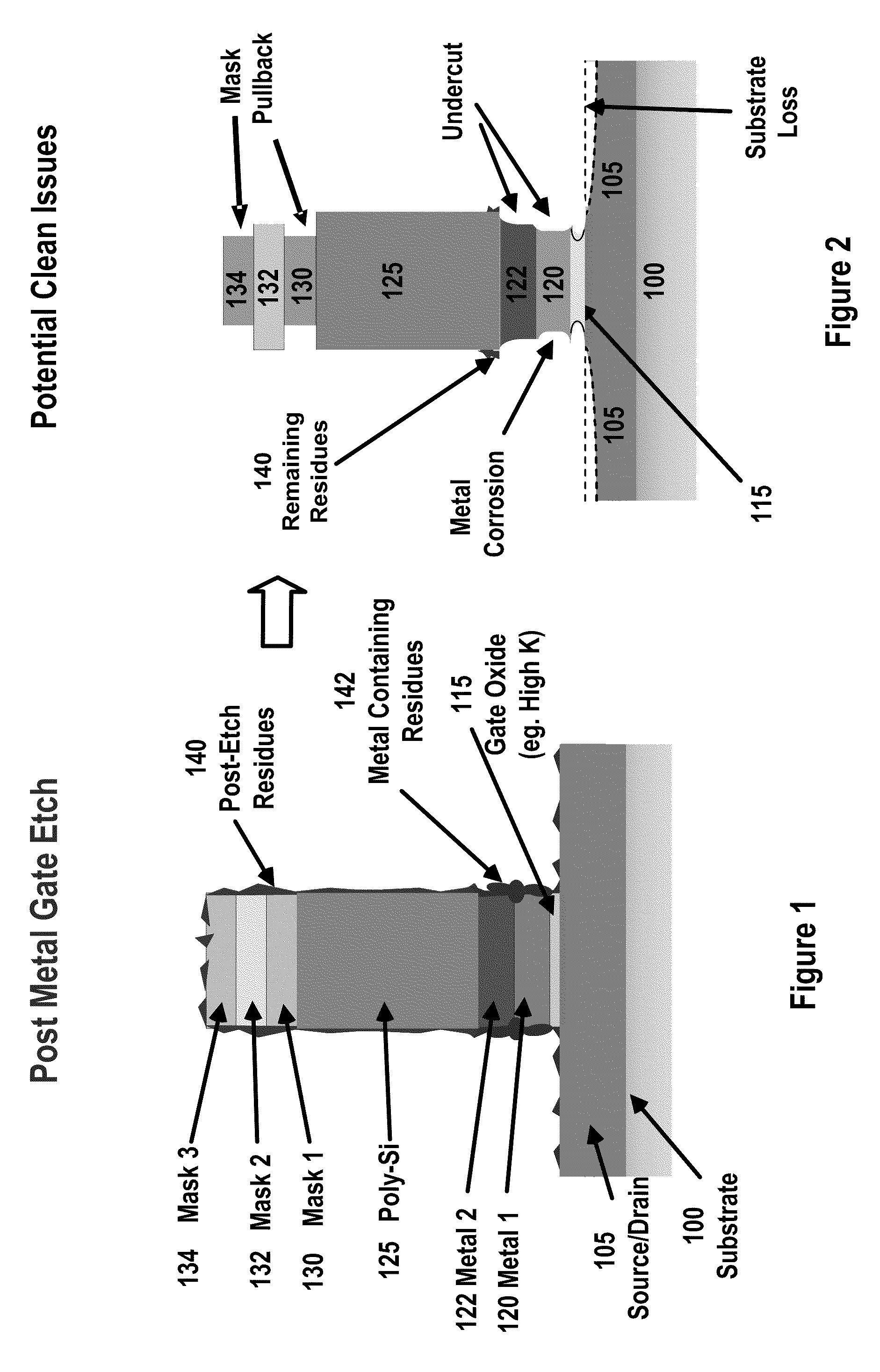
The prolonged exposure of the gate structure to aggressive cleaning chemistry used in the batch tool results in the erosion of the hardmask, otherwise known as hardmask pullback.
The hardmask erosion results in the premature exposure of the underlying layers leading to potential damage and / or further contamination of the gate features.
The prolonged exposure to the cleaning chemistry may further result in the undercut of the metal layer, such as tungsten, tungsten silicide, etc., used in forming the metal electrode over the gate oxide eventually exposing the gate oxide to the cleaning chemistry.
The pullback of the hardmask and the undercut of the metal and other layers of the gate structure including the gate oxide pose the greatest problems in the cleaning process.
The premature exposure of the various layers of a gate stack to chemistries used in subsequent fabrication operations may result in further damage of the layers lending the gate structure inoperable.
Efficient and non-damaging removal of contaminants during fabrication poses a great challenge in the cleaning process.

Method used


Image

  • Method and apparatus for surface treatment of semiconductor substrates using sequential chemical applications
  • Method and apparatus for surface treatment of semiconductor substrates using sequential chemical applications
  • Method and apparatus for surface treatment of semiconductor substrates using sequential chemical applications

Examples


Embodiment Construction

[0024]Several embodiments for effectively removing polymer residues, including metal containing polymer residues, from around a metal gate structure formed on a surface of a substrate will now be described. It will be obvious, however, to one skilled in the art, that the present invention may be practiced without some or all of these specific details. In other instances, well known process operations have not been described in detail in order not to unnecessarily obscure the present invention.

[0025]Effective removal of contaminants, such as polymer residues and metal containing polymer residues, from the surface of a substrate helps in retaining the functionality of the features formed on the substrate and the resulting devices, such as microchips. In one embodiment of the invention, the polymer residues formed around a metal gate structure are removed by sequentially applying aggressive chemistries to the surface of the substrate. The aggressive chemistries are applied in a very co...


PUM


Abstract

A system and method for removing polymer residue from around a metal gate structure formed on a surface of a substrate during a post-etch cleaning operation includes determining a plurality of process parameters associated with the metal gate structure and the polymer residue to be removed. A plurality of fabrication layers define the metal gate structure and the process parameters define characteristics of the fabrication layers and the polymer residue. A first cleaning chemistry and second cleaning chemistry are identified and a plurality of application parameters associated with the first and second cleaning chemistries are defined based on the process parameters. The first and second application chemistries are applied sequentially in a controlled manner using the application parameters to substantial remove the polymer residue while preserving the structural integrity of the gate structure.

Description

CLAIM OF PRIORITYCross Reference to Related Applications[0001]This application claims priority over U.S. Provisional application No. 61 / 083,498, filed on Jul. 24, 2008, and entitled “Method and Apparatus for Surface Treatment of Semiconductor Substrates using Sequential Chemical Applications,” which is incorporated herein by reference.FIELD OF THE INVENTION[0002]The present invention relates generally to semiconductor substrate processing, and more particularly, to systems and methods for treating a surface of a semiconductor substrate using sequential chemical applications.DESCRIPTION OF THE RELATED ART[0003]Semiconductor devices are obtained through various fabrication operations. The fabrication operations define a plurality of features, such as gate structures, on semiconductor wafers (wafers or substrates) that span multi-levels. During the various fabrication operations, the substrate is exposed to various contaminants. Any material or chemical used in the fabrication operatio...

Claims


Application Information

Patent Timeline
IPC IPC(8): B08B7/04B08B13/00
CPCH01L21/02071H01L21/6704H01L21/67075H01L21/67051H01L22/12H01L22/20H01L21/67253H01L21/18H01L21/302
Inventor MIKHAYLICHENKO, KATRINASABBA, YIZHAKPODLESNIK, DRAGAN
Owner LAM RES CORP
Learn More