Semiconductor laser device and method of manufacturing the same

a semiconductor laser and laser technology, applied in the direction of laser optical resonator construction, lasers, semiconductor lasers, etc., can solve the problems of large variation in device characteristics, low crystallinity, and inability to meet the requirements of laser operation, so as to reduce the oscillation threshold and improve the optical output efficiency of the semiconductor laser device.

Active Publication Date: 2010-01-28
LUMENTUM JAPAN INC
View PDF9 Cites 0 Cited by
  • Summary
  • Abstract
  • Description
  • Claims
  • Application Information

AI Technical Summary

Benefits of technology

[0010]An object of the present invention is to overcome the above-described problems, and to provide a semiconductor laser device manufacturing technology capable of reducing κL with manufacturing restrictions satisfied.
[0017]According to the present invention, in the semiconductor laser device having the diffraction grating, a value of κL can be reduced with manufacturing restrictions satisfied. Furthermore, with an effect that the reactive product deteriorated in crystallinity on a regrowth surface is removed, an improvement of the optical output efficiency of the semiconductor laser device and a reduction of oscillation threshold can be achieved.

Problems solved by technology

Lengthening an oscillator and reducing κ in association with the lengthening are took up as technical problems.
However, if the height of the diffraction grating is too low, large variations in yield of device characteristics, caused by deterioration in etching controllability over the diffraction grating layer or loss due to thermal decomposition at increase in temperature in burying regrowth or the like, may occur.
The product is low in crystallinity and may cause deterioration of laser device characteristics.
In this case, a shape of the diffraction grating become rectangular, and it is difficult to form a sine wave shape through etching.
In this case, however, the above-mentioned problem occurs due to mass transport.
As has been descried above, in the conventional semiconductor laser device manufacturing technology, the lower limit of height of the diffraction grating is determined by the restrictions in the diffraction grating forming process, thereby it is difficult to reduce the value of κ. Also, a reactive product is formed on side surfaces and the trench portions of the diffraction grating in a process of an increase of temperature in burying regrowth of the diffraction grating, and causes deterioration of oscillation threshold and optical output efficiency of the device.

Method used


Image

  • Semiconductor laser device and method of manufacturing the same
  • Semiconductor laser device and method of manufacturing the same
  • Semiconductor laser device and method of manufacturing the same

Examples


first embodiment

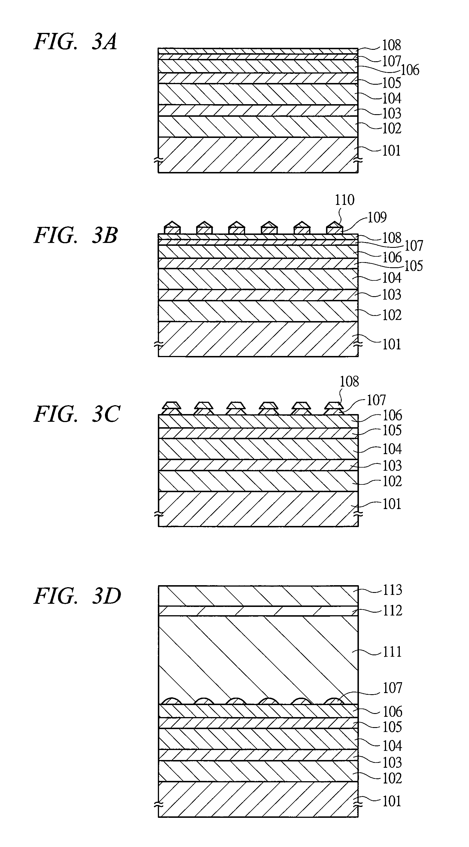
[0036]FIG. 3 is a drawing that shows a process chart of a semiconductor laser device manufacturing method according to a first embodiment of the present invention.

[0037]On an n-InP substrate 101, an n-InP first clad layer 102, an n-InGaAlAs first optical guide layer 103, an InGaAlAs active layer 104, a p-InGaAlAs second optical guide layer 105, a p-InP spacer layer 106, a p-InGaAsP diffraction grating layer 107, and a p-InP cap layer 108 are laminated through MOCVD (FIG. 3A). To enhance a carrier confinement effect, the InGaAlAs active layer 104 has an MQW configuration consisted of an InGaAlAs barrier layer and InGaAlAs well layer. Also, in consideration of controllability over a process of forming a diffraction grating, the diffraction grating layer is made to have a film thickness of 25 nm.

[0038]Next, through CVD, an insulating film 109, such as a silicon dioxide (SiO2) film or a silicon nitride (SiN) film and the like, is formed. After a resist film 110 is applied, stripes with ...

second embodiment

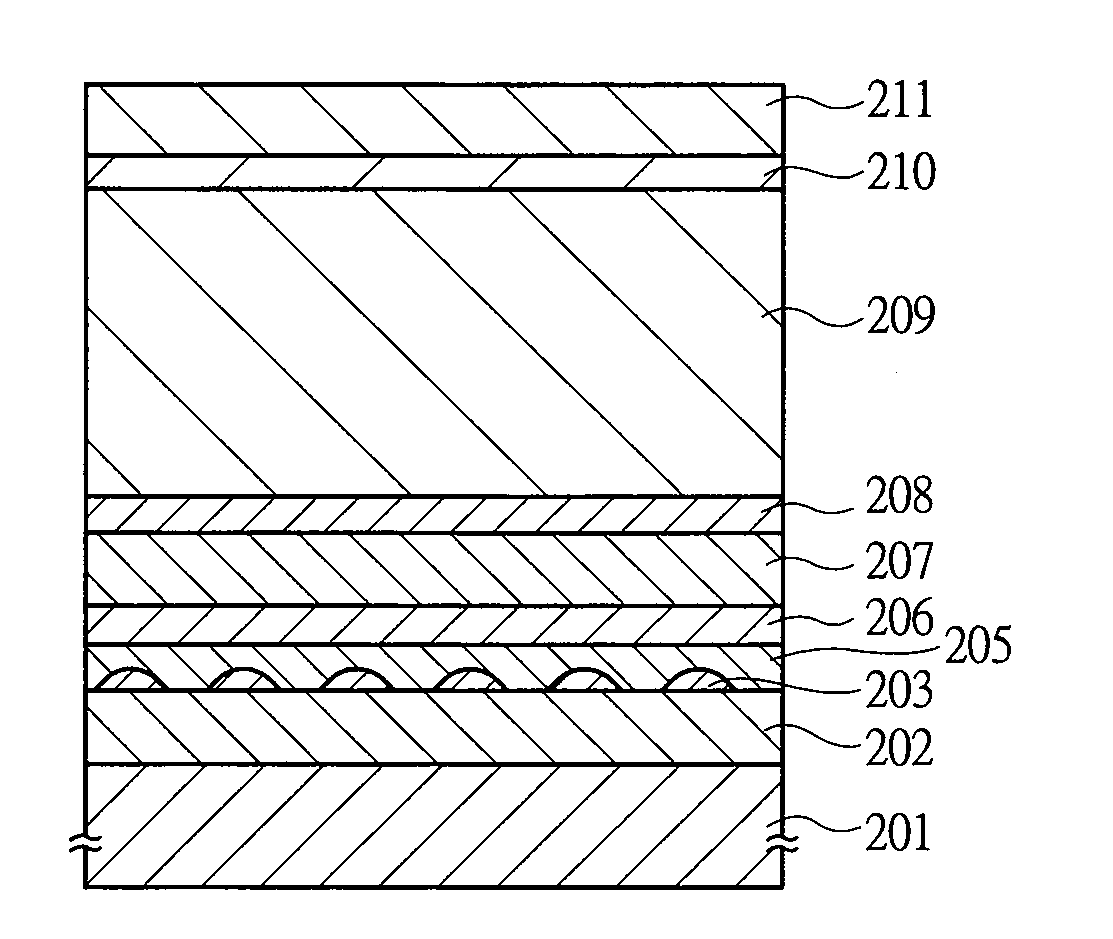
[0046]FIG. 4 is a drawing that shows a process chart of a semiconductor laser device manufacturing method according to a second embodiment of the present invention. In this embodiment, a method of manufacturing a semiconductor laser device, in which a diffraction grating is disposed on a lower side of an active layer, is described.

[0047]On an n-InP substrate 201, an n-InP first clad layer 202, an n-InGaAlAsP diffraction grating layer 203, and an n-InP cap layer 204 are laminated through MOCVD (FIG. 4A). Here, the n-InGaAsP diffraction grating layer 203 is made to have a film thickness of 25 nm, similar to that of the first embodiment.

[0048]Next, an insulating film is formed through CVD and, a diffraction grating is formed using a process similar to that of the first embodiment (FIG. 4B).

[0049]After that, through MOCVD, burying regrowth of the diffraction grating is performed. Immediately before regrowth, as with the first embodiment, halogen-based gas is supplied so that the side su...


PUM


Abstract

A method of manufacturing semiconductor laser device capable of reducing κL, with manufacturing restrictions satisfied, is provided. In a distributed-feedback or distributed-reflective semiconductor laser device, immediately before burying regrowth of a diffraction grating, halogen-based gas is introduced to a reactor, and etching is performed on the diffraction grating so that each side wall has at least two or more crystal faces and a ratio of length of an upper side in a waveguide direction to a bottom side parallel to a (100) surface is 0 to 0.3. And, a reactive product formed on side surfaces of the diffraction grating and in trench portions between stripes of the diffraction grating at an increase of temperature for regrowth is removed. Therefore, the diffraction grating with reduced height and a sine wave shape is obtained, thereby κL of the device is reduced. Thus, an oscillation threshold and optical output efficiency can be improved.

Description

CROSS-REFERENCE TO RELATED APPLICATION[0001]The present application claims priority from Japanese patent application No. JP 2006-122777 filed on Apr. 27, 2006, the content of which is hereby incorporated by reference into this application.TECHNICAL FIELD OF THE INVENTION[0002]The present invention relates to semiconductor laser devices and manufacturing techniques thereof, and particularly relates to techniques effective when applied to distributed-feedback or distributed-reflective semiconductor laser devices for optical transmission apparatuses or information storage apparatuses, and a method of manufacturing thereof.BACKGROUND OF THE INVENTION[0003]For example, as a light source for optical transmission apparatus or information storage apparatus, a distributed feedback (DFB) laser using a refractive-index-modulation diffraction grating, which has narrow spectrum and allows single mode oscillation, is mainly adopted. In a DFB laser, light output and modulation characteristic signi...

Claims


Application Information

Patent Timeline
Patent Type & Authority Applications(United States)
IPC IPC(8): H01L21/30H01S5/12
CPCB82Y20/00H01S5/12H01S5/34313H01S5/125H01S5/34306H01S5/1231
Inventor OKAMOTO, KAORUWASHINO, RYUKOMATSU, KAZUHIROSAKUMA, YASUSHI
Owner LUMENTUM JAPAN INC
Why Eureka
Try Eureka