Nonvolatile memory device, nonvolatile memory system, and access device

a non-volatile memory and access device technology, applied in pulse generators, pulse techniques, instruments, etc., can solve problems such as user being at a risk of burns, and achieve the effect of increasing the non-volatile memory device, not being at a risk of burns, and high speed

Active Publication Date: 2010-01-28
SK HYNIX INC
View PDF9 Cites 57 Cited by
  • Summary
  • Abstract
  • Description
  • Claims
  • Application Information

AI Technical Summary

Benefits of technology

[0068]In a nonvolatile memory device and a nonvolatile memory system of the present invention, an access rate control part in the nonvolatile memory device controls an access rate on the basis of a temperature of the nonvolatile memory device or a size of all data to be read and written and cools the nonvolatile memory device, thereby data reading and writing can be carried out at a high speed with temperature increase of the nonvolatile memory device in reading and writing data from and to a nonvolatile memory suppressed so that a user cannot be at a risk of a burn.
[0069]In an access device of the present invention, the data reading and writing can be carried out at a high speed with temperature increase of the nonvolatile memory device caused by reading and writing data from and to the nonvolatile memory suppressed so that a user cannot be at a risk of a burn. In addition, since an access rate is controlled by switching a bit rate or a frame rate in a case of recording a moving image, it is possible to prevent the recording from being stopped due to heat generation.

Problems solved by technology

However, when data is read or written at a high speed, surface temperatures of a host device and a semiconductor memory card become exceedingly high in general, and thereby a user is at a risk of a burn when ejecting the semiconductor memory card from the host device.

Method used


Image

  • Nonvolatile memory device, nonvolatile memory system, and access device
  • Nonvolatile memory device, nonvolatile memory system, and access device
  • Nonvolatile memory device, nonvolatile memory system, and access device

Examples


first embodiment

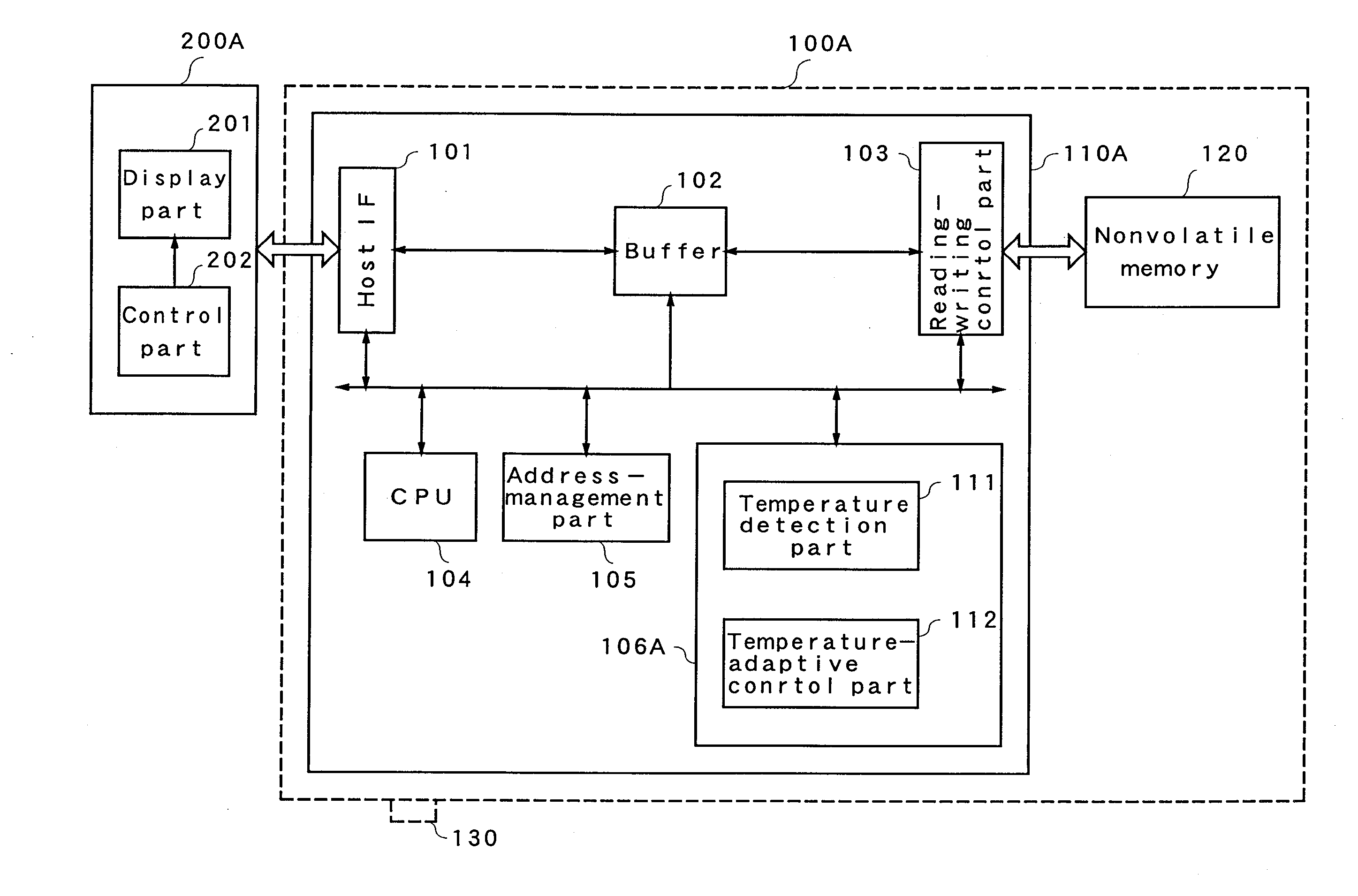
[0144]FIG. 1 is a block diagram showing a nonvolatile memory system according to a first embodiment of the present invention. As shown in FIG. 1, the nonvolatile memory system of the present embodiment is configured by including a nonvolatile memory device 100A and an access device 200A to which the nonvolatile memory device 100A is attached.

[0145]Firstly, the access device 200A includes: a display part 201 for displaying information related to the nonvolatile memory system; and a control part 202. The control part 202 accesses the nonvolatile memory device 100A to write and read data, and carries out a control to display necessary information of information received from the nonvolatile memory device 100A.

[0146]Next, the nonvolatile memory device 100A will be explained. As shown in FIG. 1, the nonvolatile memory device 100A includes a memory controller 110A, a nonvolatile memory 120 that is a flash memory group, and a mode changeover switch 130. The mode changeover switch 130 is a ...

second embodiment

[0186]FIG. 12 is a block diagram showing a nonvolatile memory system according to a second embodiment of the present invention. As shown in FIG. 12, the nonvolatile memory system on the present embodiment is configured by including a nonvolatile memory device 100B, and an access device 200B to which the nonvolatile memory device 100B is attached.

[0187]A memory controller 110B of the nonvolatile memory device 100B includes an access rate control part 106B. Further, the access rate control part 106B includes a status information generation part 113. In the present embodiment, components other than the status information generation part 113 are the same as those of the first embodiment and are shown by the same numerals as those of the first embodiment.

[0188]On the other hand, the access device 200B has a control part 203 and a cooling part 204 in addition to the display part 201. The control part 203 controls an access to the nonvolatile memory device 100B on the basis of status infor...

third embodiment

[0205]FIG. 15 is a block diagram showing a nonvolatile memory system according to a third embodiment of the present invention. The nonvolatile memory system of the present embodiment is configured by including a nonvolatile memory device 100C and the access device 200A. A memory controller 110C of the nonvolatile memory device 100C includes a temperature calculation part 114 in an access rate control part 106C. The temperature calculation part 114 does not use a sensor such as a thermistor but obtains the temperature T of the nonvolatile memory device 100C in accordance with the approximate calculation based on expressions (5-1) or (5-3) explained in the second embodiment. In the present embodiment, the access device 200A and the nonvolatile memory device 100C are the same as those of the first embodiment except the temperature calculation part 114, and are shown by the same numerals as those of the first embodiment. Additionally, in this approximate calculation, the environmental t...


PUM


Abstract

When an access device accesses a nonvolatile memory device, the nonvolatile memory device or the access device detects or calculates a temperature T of the nonvolatile memory device. A temperature-adaptive control part of the nonvolatile memory device controls an access rate to a nonvolatile memory on the basis of the temperature T. Accordingly, the control part controls the rate so that the temperature T of the nonvolatile memory devices cannot exceed a limit temperature Trisk. In this manner, a nonvolatile memory system can eliminate a risk of a burn when ejecting the semiconductor memory device and can read and write data at a high speed.

Description

TECHNICAL FIELD[0001]The present invention relates to: a nonvolatile memory device having a semiconductor memory such as a semiconductor memory card; an access device for accessing the nonvolatile memory device; and a nonvolatile memory system including them.BACKGROUND ART[0002]A nonvolatile memory device having a rewritable nonvolatile memory is increasingly demanded mainly for a semiconductor memory card. The semiconductor memory card is high-price compared to an optical disk, a tape medium, and the like. The semiconductor memory card, however, is increasingly demanded as a recording medium for a portable apparatus such as a digital still camera and a mobile phone because of merits such as small-size, lightweight, vibration resistance, and easy handling, and is used for not only a consumer-use moving image recording apparatus but also a professional-use moving image recording apparatus. In addition, not only the portable apparatus but also a stationary apparatus such as a digital ...

Claims


Application Information

Patent Timeline
Patent Type & Authority Applications(United States)
IPC IPC(8): G06F12/00H01L35/00
CPCG06F1/206G11C16/102G11C7/04
Inventor NAKANISHI, MASAHIROKATO, ISAOTOYAMA, MASAYUKIADACHI, TATSUYANAKAGAKI, HIROFUMIMAEDA, TAKUJI
Owner SK HYNIX INC
Why Eureka
Try Eureka