

Semiconductor device and production method thereof
- Summary
- Abstract
- Description
- Claims
- Application Information
AI Technical Summary
Benefits of technology
Problems solved by technology
Method used
Image

Examples
embodiment 1
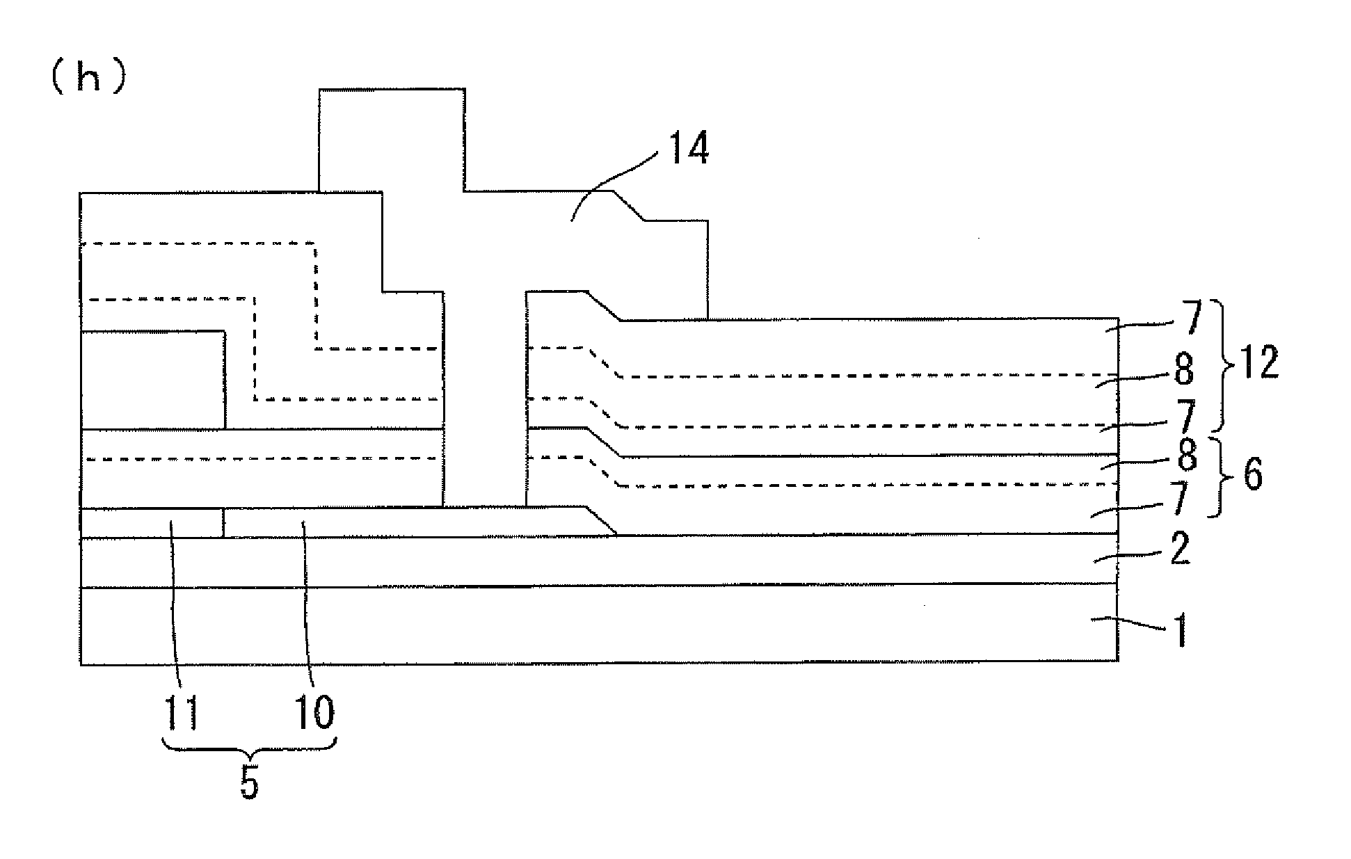
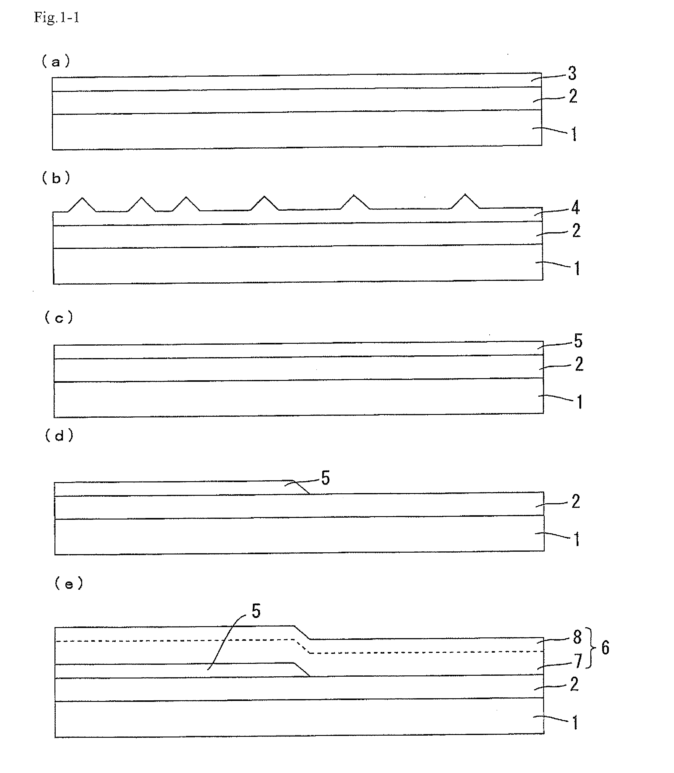
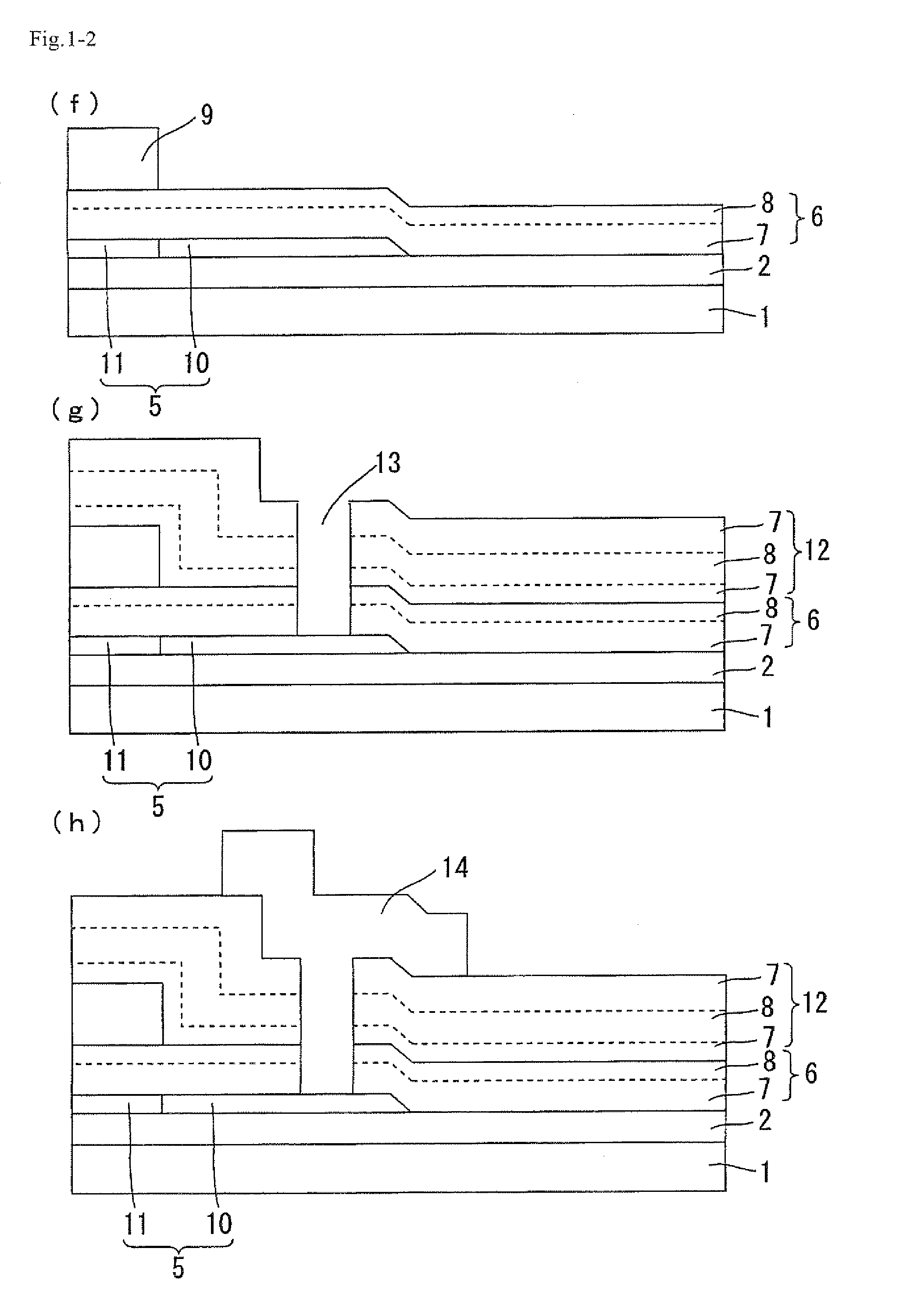
[0026]A method for producing a thin film transistor (TFT) in Embodiment 1 in accordance with a semiconductor device of the present invention is mentioned below with reference to FIG. 1. FIGS. 1-1(a) to (e) and FIGS. 1-2(f) to (h) are cross-sectional views schematically showing a production flow of the TFT in the present Embodiment. FIGS. 1-1 and 1-2 are cross-sectional views schematically showing the TFT in the channel length direction. The TFT in the present Embodiment has a substantially symmetric structure in the channel length direction. Therefore, FIGS. 1-1 and 1-2 show the structure on only one side of the TFT.
[0027]As shown in FIG. 1-1(a), on a glass substrate 1 that is an insulating substrate, a base coat (EC) layer 2 was first formed by a plasma CVD method and the like, and successively an amorphous silicon (a-Si) film 3 was formed to have a thickness of 50 nm. Examples of the BC layer 2 include a silicon oxide (SiO2) film, a silicon nitride film (SiNx) film, and a silicon ...
experiment 1
“Experiment 1”
Verification of Gate Leakage Current (Ig) Characteristics and Breakdown Voltage Relative to Gate Voltage (Vg)
[0039]FIG. 2 is a graph showing gate leakage current (Ig) characteristics and breakdown voltage relative to gate voltage (Vg) of the TFTs in Embodiment 1 and Comparative Embodiments 1 to 3. The following Table 1 shows comparative results of the breakdown voltage of the TFTs in Embodiment 1 and Comparative Embodiments 1 to 3. The results show that in the TFT in Embodiment 1 of the present invention, a remarkable reduction in gate leakage current and remarkable improvement in withstand voltage were observed, which can not be anticipated by the results in the cases where the treatment of flattening the p-Si film and the formation of the gate insulating film having a multilayer structure are singly performed. It appears that this can be realized because, in the TFT in Embodiment 1, the gate insulating film has excellent coverage for the upper and end parts of the p-...
experiment 2
“Experiment 2”
Verification of Shift in Threshold (ΔVth) Before and After Applying the Gate Bias Stress Voltage
[0040]FIG. 3 is a graph showing a shift in threshold (AVth) before and after applying the gate bias stress voltage to the TFTs in Embodiment 1 and Comparative Embodiment 3 in which the gate insulating film has a multilayer structure. The shift in threshold (AVth) was calculated by subtracting the threshold before the application from the threshold after applying the gate bias stress voltage for 10 sec. In the present Experiment, N-type TFTs were produced in Embodiment 1 and Comparative Embodiment 3 and the present Experiment was performed. As shown in FIG. 3, the reliability was improved in the TFT in Embodiment 1 in which the p-Si film was flattened because the shift in threshold accompanied with the application of the gate bias stress was reduced to half or less the shift in threshold of the TFT in Comparative Embodiment 3 in which the p-Si film was unflattened. This shows...
PUM
 Abstract
Description
Claims
Application Information