Trench type semiconductor device and fabrication method for the same

Active Publication Date: 2010-02-04
ROHM CO LTD
View PDF19 Cites 42 Cited by
  • Summary
  • Abstract
  • Description
  • Claims
  • Application Information

AI Technical Summary

Benefits of technology

[0015]According to the present invention, the trench type semiconductor device which achieves the minute structure by the self-alignment, reduces the on resistance, and improves the breakdown capability, and the fabrication method for the trench type semiconductor device can be provided.
[0016]According to the present invention, the interlayer insulating film includes the impurity consisting of

Problems solved by technology

Accordingly, there was a subject that it is not easy to apply thickness of the level that the polysilicon gate can be insulated by the local oxidation film.
In order to make the local oxidation film into the thickness which can be insulated in this way, although the method of heat treatment of high temperature or long duration can be considered, another problem of degrading the element characteristic of the fabricated MOS transistor occ

Method used


Image

  • Trench type semiconductor device and fabrication method for the same
  • Trench type semiconductor device and fabrication method for the same
  • Trench type semiconductor device and fabrication method for the same

Examples


first embodiment

(Element Structure)

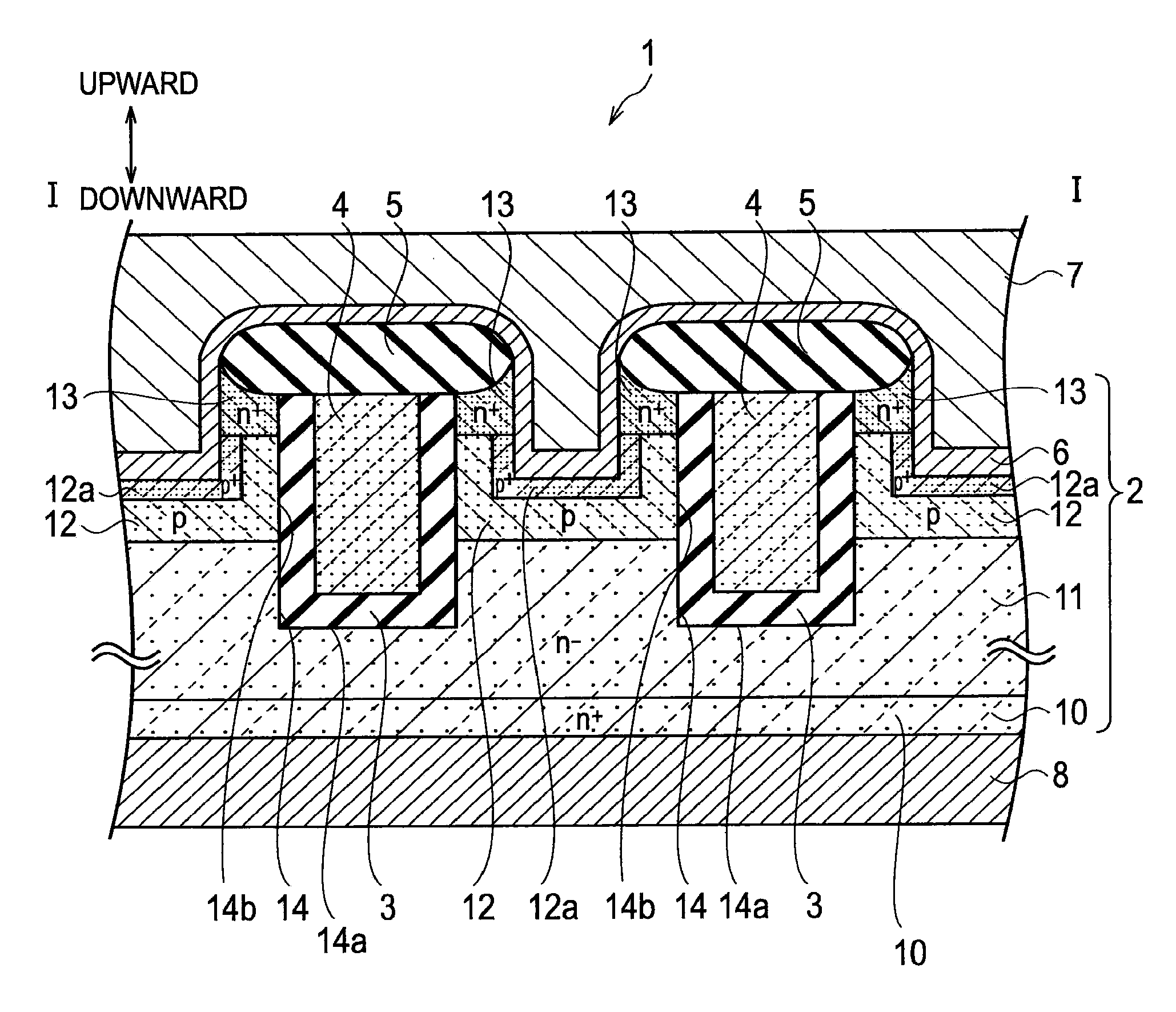
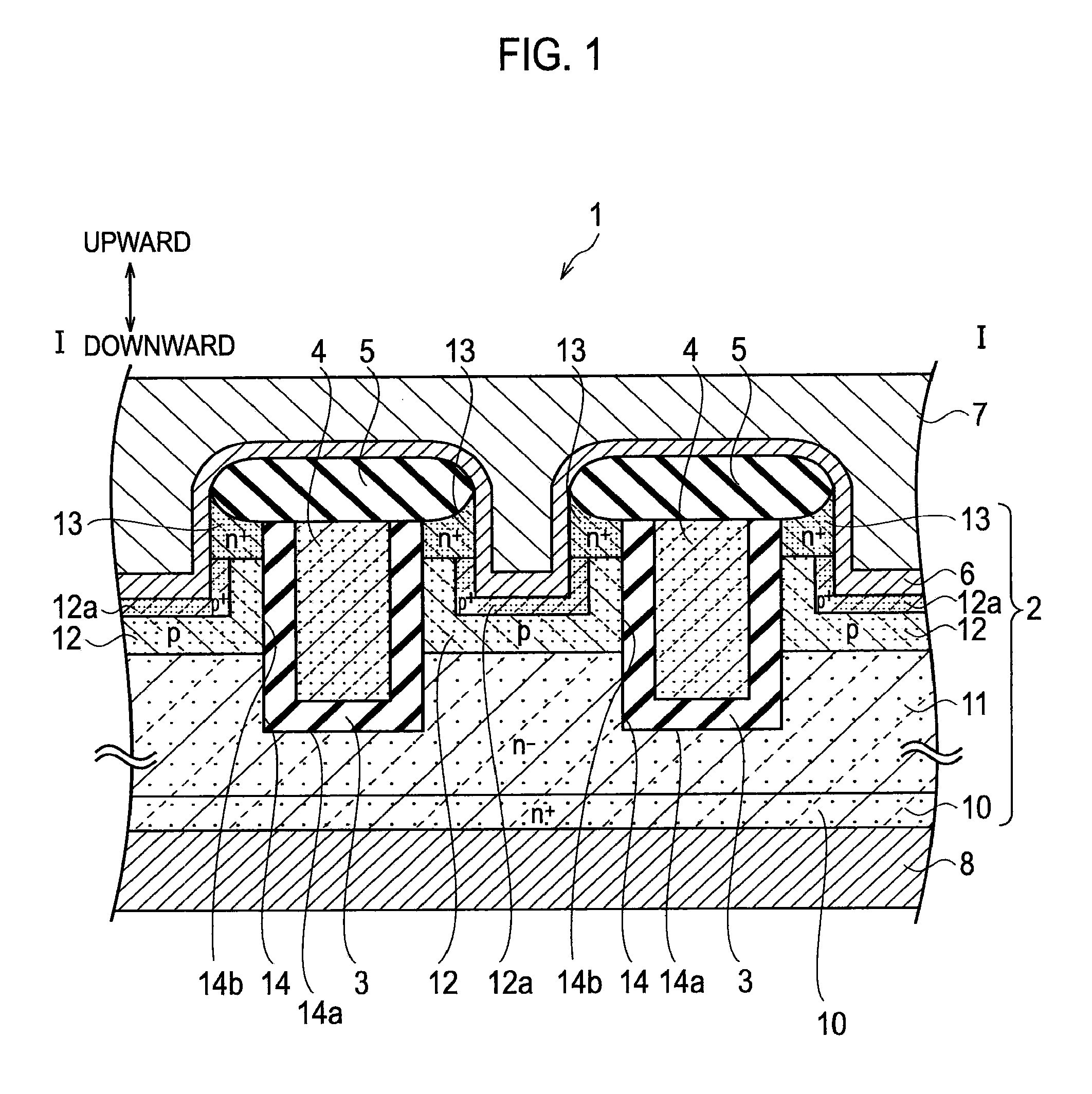
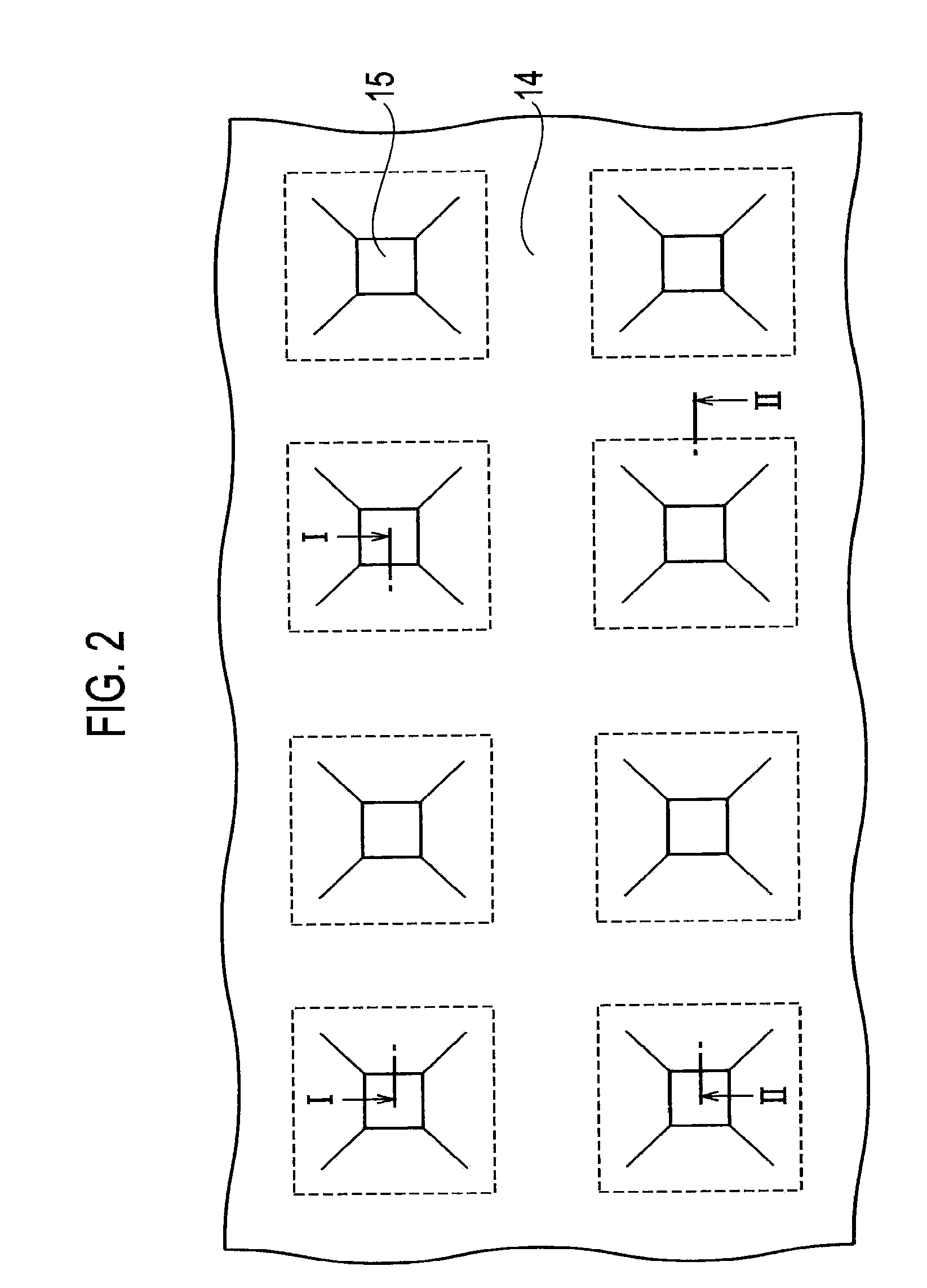
[0051]A schematic cross-section structure of a trench type semiconductor device according to a first embodiment of the present invention is expressed as shown in FIG. 1. Moreover, a lattice-like plane pattern configuration of the trench type semiconductor device according to the first embodiment is expressed as shown in FIG. 2. FIG. 1 corresponds to the schematic cross-section structure taken in the line I-I of FIG. 2.

[0052]As shown in FIG. 1, the trench type semiconductor device according to the first embodiment of the present invention includes: a n− type first base layer 11; a gate insulating film 3 placed on a bottom surface 14a and a sidewall surface 14b of a trench 14 formed from the surface of the n− type first base layer 11; a gate electrode 4 which is placed on the gate insulating film 3 and fills up into the trench 14; an interlayer insulating film 5 which is placed by covering the gate electrode 4; a p type second base layer 12 which is placed on the su...

second embodiment

[0121]Hereinafter, a second embodiment which applies the present invention to the MOSFET with reference to drawings will be described. FIG. 19 is a schematic cross-sectional configuration diagram of a trench type semiconductor device 1 according to the second embodiment. In addition, upward and downward shown by the arrow of FIG. 19 is applied as the up-and-down direction of the trench type semiconductor device 1.

[0122]As shown in FIG. 19, the trench type semiconductor device 1 according to the second embodiment includes a substrate 2, a gate insulating film 3, a gate electrode 4, an interlayer insulating film 5, a barrier metal layer 6, a source electrode 7, and a drain electrode 8.

[0123]The substrate 2 makes n− type silicon as a main constituent.

[0124]A n− type first base layer 11 is formed in the drain electrode 8 side of the substrate 2.

[0125]A p− type second base layer 12 is formed in the intermediate layer of the substrate 2. The p− type second base layer 12 has the thickness ...


PUM


Abstract

The trench type semiconductor device includes a gate insulating film placed on the bottom surface and the sidewall surface of the trench formed from the surface of a first base layer; a gate electrode placed on the gate insulating film and fills up into a trench; an interlayer insulating film covering the gate electrode; a second base layer placed on the surface of the first base layer, and is formed more shallowly than the bottom surface of the trench; a source layer placed on the surface of the second base layer; a source electrode connected to the second base layer in the bottom surface of a self-aligned contact trench formed in the second base layer by applying the interlayer insulating film as a mask, and is connected to the source layer in the sidewall surface; a drain layer placed at the back side of the first base layer; and a drain electrode placed at the drain layer, for achieving the minute structure by the self-alignment, reducing the on resistance, and improving the breakdown capability, and providing a fabrication method for the same.

Description

CROSS REFERENCE TO RELATED APPLICATIONS AND INCORPORATION BY REFERENCE[0001]This application is based upon and claims the benefit of priority from prior Japanese Patent Applications No. P2008-194805 filed on Jul. 29, 2008, and No. P2008-229028 filed on Sep. 5, 2008, the entire contents of which are incorporated herein by reference.TECHNICAL FIELD[0002]The present invention relates to a trench type semiconductor device and a fabrication method for the trench type semiconductor device. More specifically, the present invention relates to a trench type semiconductor device which achieves minute structure by a fully self-aligned, reduces the on resistance, and improves breakdown capability, and a fabrication method for the same.BACKGROUND ART[0003]Conventionally, trench type semiconductor devices, such as a vertical MOSFET (Metal Oxide Semiconductor Field Effect Transistor) and IGBT (Insulated Gate Bipolar Transistor) with which a trench is formed in a substrate and a gate electrode is f...

Claims


Application Information

Patent Timeline
IPC IPC(8): H01L29/78H01L21/336
CPCH01L29/0653H01L29/0696H01L29/0878H01L29/7813H01L29/41766H01L29/456H01L29/66734H01L29/1095
Inventor YOSHIMOCHI, KENICHI
Owner ROHM CO LTD
Why Eureka
Try Eureka