Transparent electrode for display device and manufacturing method thereof

Inactive Publication Date: 2010-02-11
KOBE STEEL LTD
View PDF39 Cites 30 Cited by
  • Summary
  • Abstract
  • Description
  • Claims
  • Application Information

AI Technical Summary

Benefits of technology

[0033]The present invention is configured as described above. Therefore, it is possible to obtain a transparent electrode for a display device having a low contact resistance with less variance (variation), and a high transmittance, even when the transparent electrode is in direct contact with the aluminum alloy film.
[0034]The effect by the present invention is exerted when the amo

Problems solved by technology

Al for use as a wiring material for a transparent electrode is very susceptible to oxidation.
However, when the Al oxide layer is formed as described above, electric ohmic connection cannot be carried out.
Specifically, a deposition device including deposition chambers for barrier metal formation respectively additionally mounted therein (typically, a cluster tool in which a plurality of deposition chambers are connected to a transfer chambe

Method used


Image

  • Transparent electrode for display device and manufacturing method thereof
  • Transparent electrode for display device and manufacturing method thereof
  • Transparent electrode for display device and manufacturing method thereof

Examples


Example

Examples

[0139]Below, the present invention will be more specifically described by way of examples. However, it is naturally understood that the present invention is not limited by the following examples, and can be carried out with proper changes within the scope adaptable to the gist described above and later. All of these are intended to be embraced by the technical scope of the present invention

Example

Example 1

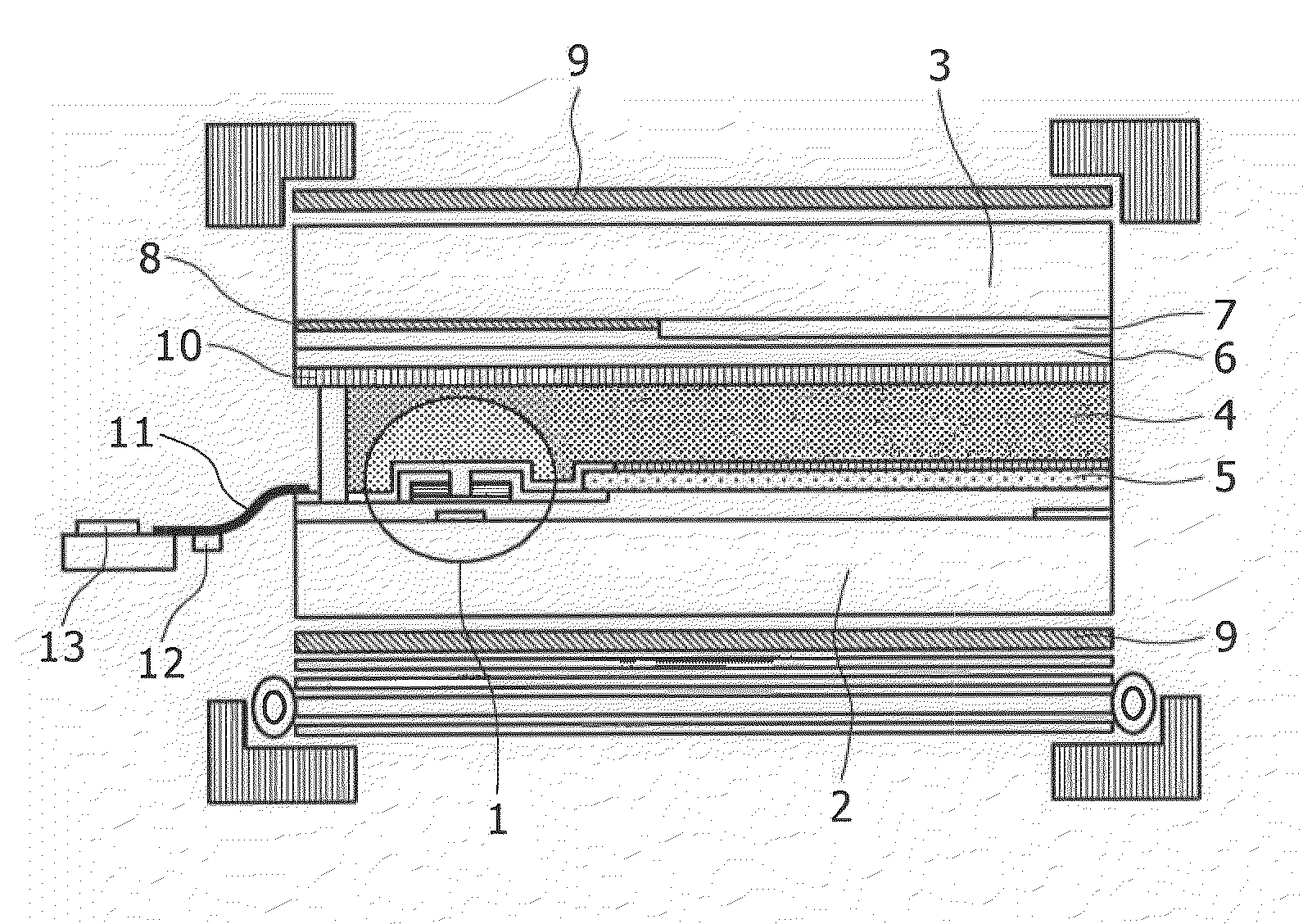
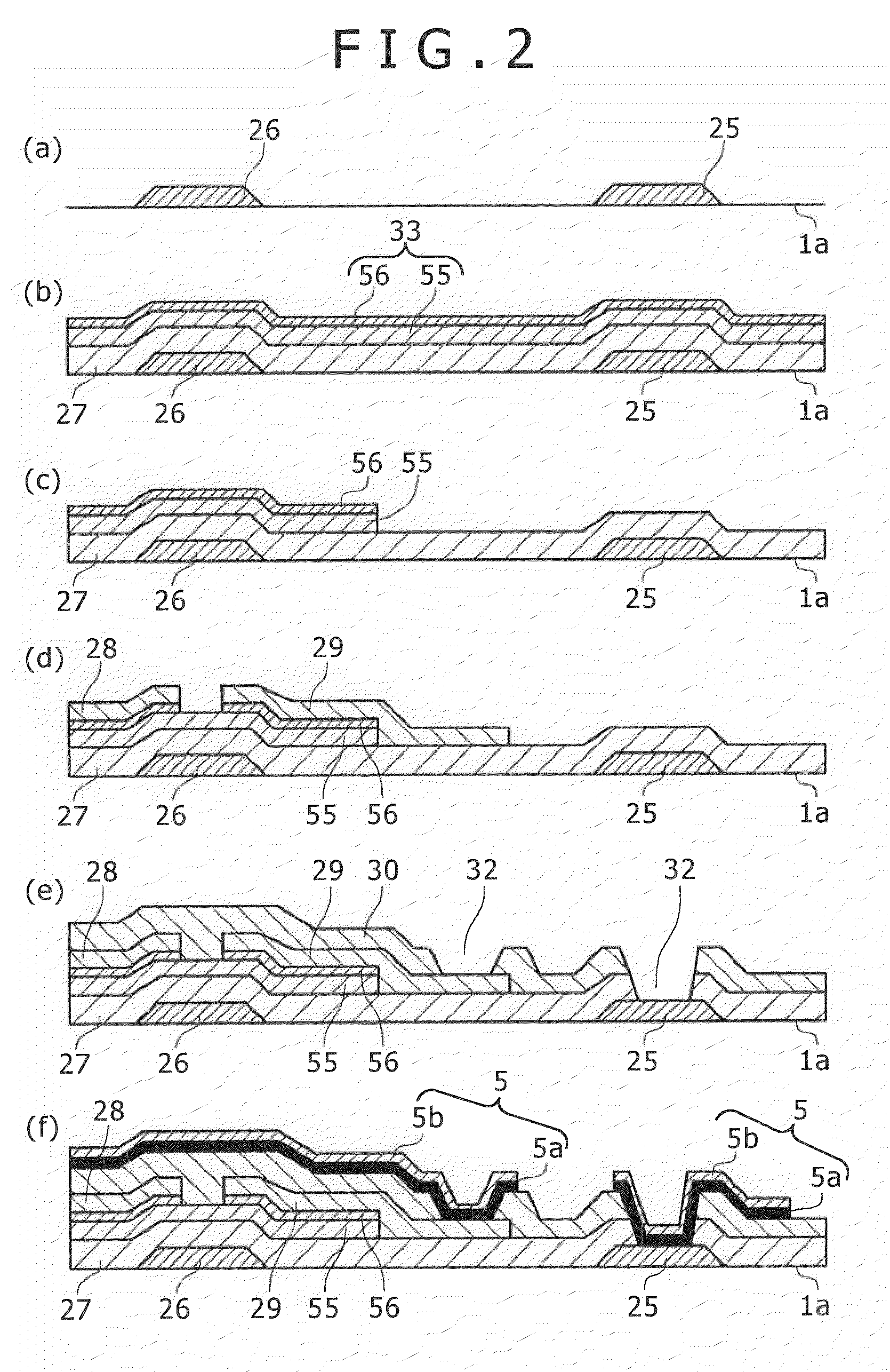
[0140]In this example, it will be verified that use of the transparent electrode of the present invention can control the contact resistivity low, and also the variance small. Specifically, there were examined changes in contact resistivity upon changing the nitrogen content in the nitrogen-containing transparent conductive film by using a test device shown in FIG. 1B, and changing the ratio (F2 / F1) of the flow rate F2 of a nitrogen gas to the flow rate F1 of a mixed gas (Ar+N2) of an inert gas (Ar) and a nitrogen gas within the range of 0 to 0.15. Herein, as the transparent conductive film, an ITO film was used, and as the aluminum alloy film, an Al-0.3 at % Ni-0.35 at % La alloy was used.

[0141]First, on a glass substrate, a 30 nm-thick Al-0.3 at % Ni-0.35 at % La alloy film was deposited by a sputtering process in the following manner.

[0142]Target material: a sputtering target of Al-0.3 at % Ni-0.35 at % La is used (size: diameter 100 mm×thickness 5 mm);

[0143]Sputtering ...

Example

Example 2

[0163]In this example, there were examined the mean value and the variance of the contact resistivities when various aluminum alloy films shown in Table 1 were used. Specifically, the contact resistivities were examined in the same manner as in Example 1, except that an IZO film was used as the transparent conductive film, and the gas flow rate ratios (F2 / F1) were set at 0 and 0.1 in Example 1. All of the aluminum alloy films shown in Table 1 are preferably used as the materials for direct contact.

[0164]These results are described together in Table 1. Herein, the nitrogen contents in the IZO film containing nitrogen (first transparent conductive film, IZO: N) when the gas flow rate ratios (F2 / F1)=0 and 0.1 are 0 at % and 2.3 at %, respectively.

TABLE 1Gas flow rateGas flow rateratio = 0ratio = 0.1ContactContactComposition of Al alloyresistivityVarianceresistivityVarianceNo.film(Ω· cm2)(Ω· cm2)(Ω· cm2)(Ω· cm2)1Al—0.3at % Ni—0.35at % La2.7E−046.E−042.1E−042.E−042Al—0.3at % Ni...


PUM

PropertyMeasurementUnit
Thicknessaaaaaaaaaa
Thicknessaaaaaaaaaa
Thicknessaaaaaaaaaa

Abstract

The present invention relates to a transparent electrode for a display device which includes a first transparent conductive film containing nitrogen, and a second transparent conductive film not containing nitrogen, wherein the first transparent conductive film is in contact with an aluminum alloy film. In accordance with the present invention, there is obtained a transparent electrode for a display device which is capable of, even when a barrier metal layer to be generally provided between an aluminum alloy film and the transparent electrode is omitted, controlling the variance small while keeping the low contact resistance, and further which is also excellent in light transmission characteristics.

Description

TECHNICAL FIELD[0001]The present invention relates to a transparent electrode for a display device, and a manufacturing method thereof. More particularly, it relates to an improved technology of a transparent electrode for a display device in which the transparent conductive film forming the transparent electrode is in direct contact with an aluminum alloy film for use in source-drain electrodes, reflection electrodes, and the like.BACKGROUND ART[0002]In recent years, with a progress of the development of liquid crystal displays, liquid panels with a screen size of more than 100 inches have come to be manufactured. The 30- to 40-inch diagonal liquid crystal display-mounted TVs have also been mass produced, which has created a strong demand for reduction of manufacturing cost thereof. Of liquid crystal displays for TVs and personal computers, those of an active panel type having a structure in which one transistor is disposed for each pixel have been the mainstream because of high op...

Claims


Application Information

Patent Timeline
IPC IPC(8): H01B5/00H05K1/09C23C14/34
CPCH01L27/124G02F1/13439
Inventor GOTOU, HIROSHIOKUNO, HIROYUKI
Owner KOBE STEEL LTD
Why Eureka
Try Eureka