Indium tin oxide (ITO) layer forming

a technology indium tin oxide, which is applied in the field of indium tin oxide (ito) layer formation, can solve the problems that the high-temperature process may not be suitable for some applications, and achieve the effect of limiting the temperature increase of the substra

Active Publication Date: 2010-02-11
APPLE INC
View PDF21 Cites 40 Cited by
  • Summary
  • Abstract
  • Description
  • Claims
  • Application Information

AI Technical Summary

Benefits of technology

[0004]This relates to forming a crystalline ITO layer on top of a substrate by heating ITO to a high temperature while limiting a temperature increase of the substrate to less than a predetermined temperature. For example, a layer including amorphous ITO may be deposited on top of the substrate, and a surface anneal process may be used to cause the ITO to undergo a phase conversion from amorphous ITO to crystalline ITO. In the surface anneal process, energy is applied in such a way that most of the energy is absorbed by the layer including amorphous ITO, and not the substrate. For example, the amorphous ITO layer may be exposed to laser light, ultraviolet (UV) radiation, microwave radiation, or other electromagnetic (EM) radiation. The wavelength of the radiation can be chosen such that the amorphous ITO layer absorbs most of the energy of the radiation. In this way, for example, the amorphous ITO layer may be sufficiently heated to undergo the phase conversion to crystalline ITO while the temperature increase of the substrate can be limited to less than a predetermined temperature, since most of the energy is absorbed by the ITO layer. In another example, energy absorption can be focused on the ITO layer by applying an electrical current to the ITO layer. The electrical resistance of the ITO layer causes some of the energy of the electrical current to be absorbed by the ITO layer in the form of heat. Focusing the flow of the electrical current through the ITO layer can allow most of the energy to be absorbed by the amorphous ITO layer, thus heating the ITO to high temperature and causing phase conversion to crystalline ITO, while limiting the temperature increase of the substrate.

Problems solved by technology

Conventional processes for depositing high-quality, crystalline ITO can require a substrate to be exposed to sustained temperatures as high as 350 degrees C. However, such high-temperature processes may not be suitable for some applications.

Method used


Image

  • Indium tin oxide (ITO) layer forming
  • Indium tin oxide (ITO) layer forming
  • Indium tin oxide (ITO) layer forming

Examples


Embodiment Construction

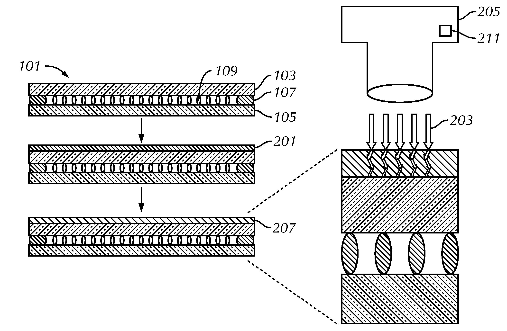
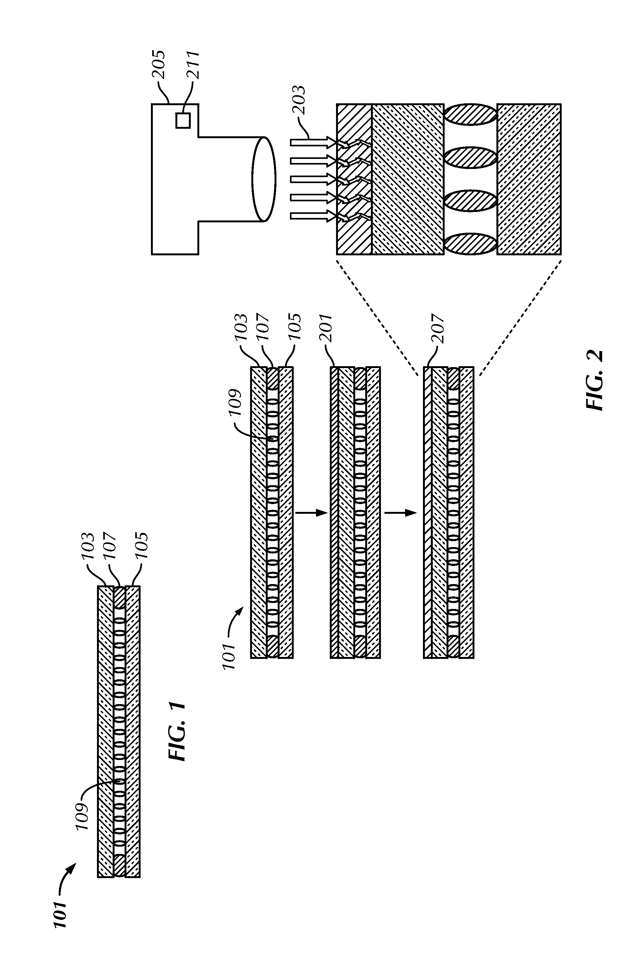
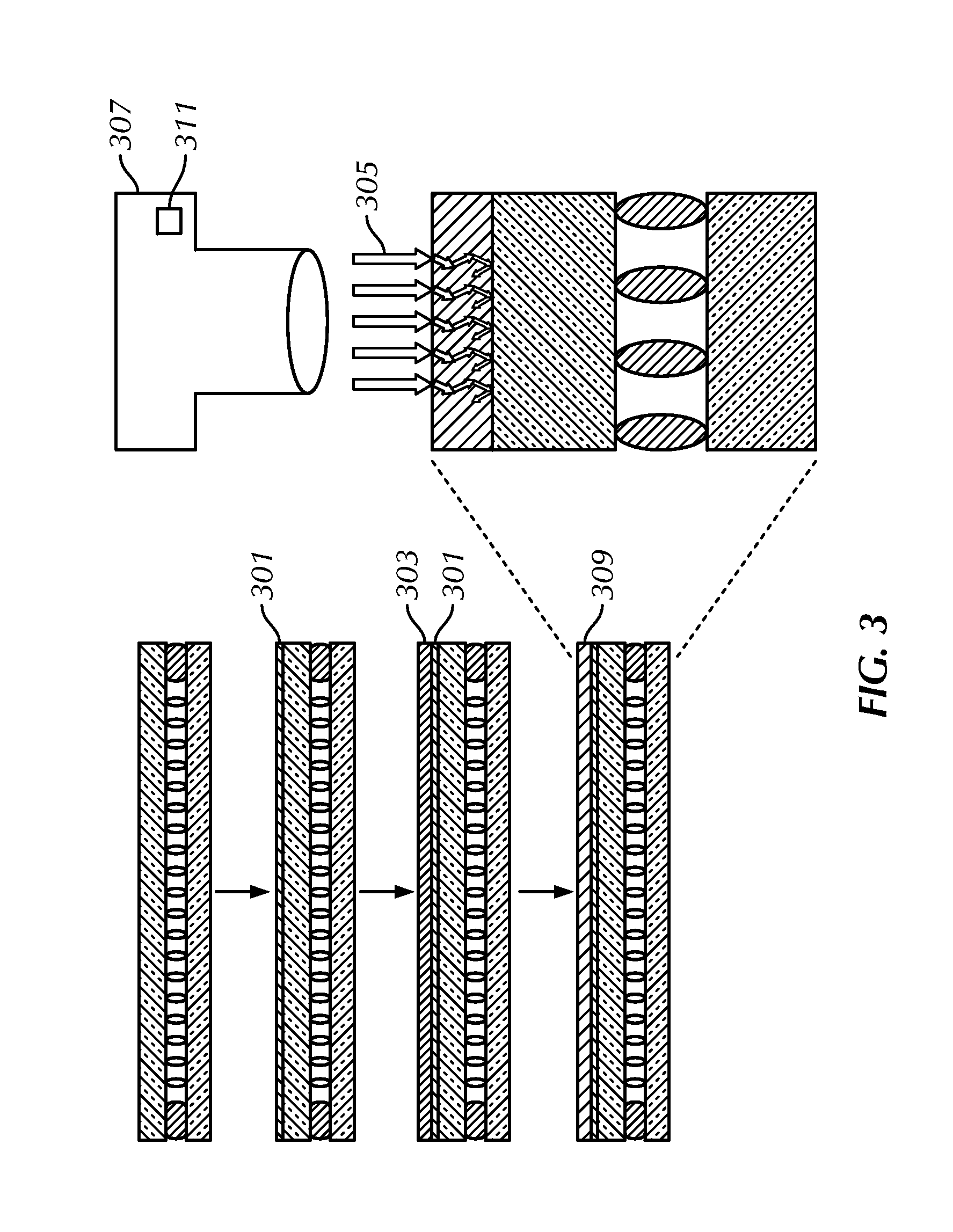
[0023]In the following description of preferred embodiments, reference is made to the accompanying drawings which form a part hereof, and in which it is shown by way of illustration specific embodiments in which the invention can be practiced. It is to be understood that other embodiments can be used and structural changes can be made without departing from the scope of the embodiments of this invention.

[0024]This relates to forming a crystalline ITO layer on top of a substrate by heating ITO to a high temperature while limiting a temperature increase of the substrate to less than a predetermined temperature. For example, a layer including amorphous ITO may be deposited on top of the substrate, and a surface anneal process may be used to cause the ITO to undergo a phase conversion from amorphous ITO to crystalline ITO. The layer including amorphous ITO may be, for example, a layer including both amorphous ITO and crystalline ITO. In the surface anneal process, energy is applied in s...


PUM

PropertyMeasurementUnit
thicknessaaaaaaaaaa
thicknessaaaaaaaaaa
sheet resistanceaaaaaaaaaa

Abstract

A layer of material, such as crystalline indium tin oxide (ITO), is formed on top of a substrate by heating the material to a high temperature, while a temperature increase of the substrate is limited such that the temperature of the substrate does not exceed a predetermined temperature. For example, a layer including amorphous ITO can be deposited on top of the substrate, and the amorphous layer can be heated in a surface anneal process using radiation while limiting substrate temperature. Another process can pass electrical current through the amorphous ITO. In another process, the substrate is passed through a high-temperature deposition chamber quickly, such that a portion of a layer of crystalline ITO is deposited, while the temperature increase of the substrate is limited.

Description

FIELD OF THE INVENTION[0001]This relates generally to the formation of indium tin oxide (ITO) layers, and in particular, forming a crystalline ITO layer on top of a substrate by heating ITO to high temperature while limiting a temperature increase of the substrate.BACKGROUND OF THE INVENTION[0002]Many types of input devices are presently available for performing operations in a computing system, such as buttons or keys, mice, trackballs, joysticks, touch sensor panels, touch screens and the like. Touch screens, in particular, are becoming increasingly popular because of their ease and versatility of operation as well as their declining price. Touch screens can include a touch sensor panel, which can be a clear panel with a touch-sensitive surface, and a display device such as a liquid crystal display (LCD) that can be positioned partially or fully behind the panel so that the touch-sensitive surface can cover at least a portion of the viewable area of the display device. Touch scree...

Claims


Application Information

Patent Timeline
Patent Type & Authority Applications(United States)
IPC IPC(8): B32B3/00B32B9/00B05D7/00B05C11/00C23C16/44B32B17/06
CPCC23C14/086C23C14/5806C23C14/5813G02F1/1303G02F1/13338G02F2001/133388Y10T428/24851G02F2201/38G06F3/0412G06F3/044H01L31/1884Y02E10/50Y10T428/24926G02F2201/122G06F3/0446G06F3/0445G02F1/133388
Inventor HUANG, LILIZHONG, JOHN Z.
Owner APPLE INC
Why Eureka
Try Eureka