Nonvolatile nanotube programmable logic devices and a nonvolatile nanotube field programmable gate array using same

a nonvolatile nanotube and gate array technology, applied in the field of field programmable devices, can solve the problems of inefficient programmable architecture, significant propagation delay, and difficult manufacturing of field programmable plas

Active Publication Date: 2010-02-18
NANTERO
View PDF78 Cites 48 Cited by
  • Summary
  • Abstract
  • Description
  • Claims
  • Application Information

AI Technical Summary

Benefits of technology

[0071]In one aspect the present disclosure relates to an integrated three-dimensional semiconductor system that can include a base level comprising a substrate, at least one level above the substrate that can include an insulating layer and at least one nanotube field effect transistor on the insulating layer. Each nanotube field effect transistor can include a nanotube fabric having a plurality of semiconducting nanotubes, the nanotube fabric having a source region and a drain region, wherein the source region and drain region are in a spaced relation relative to one another and wherein the spaced relation defines a channel region in the nanotube fabric, and a gate element electrically coupled to the channel region, wherein the gate element modulates the conductivity of the channel region such that a conductive pathway is formed or unformed between the source and drain in response to electrical stimulus.

Problems solved by technology

Thus, PROMs are an inefficient architecture for programmable logic function and are rarely used for this purpose and are therefore not included in block diagram 100.
However, for field programmable PLAs with two memory arrays (memory planes) requiring electrically programmable AND and OR arrays, field programmable PLAs were difficult to manufacture and introduced significant propagation delays.
The difficulty of increasing capacity of a single SPLD architecture is that the array size of the programmable logic-arrays are driven to large dimensions as the number of inputs increase.
The result is less architectural flexibility and smaller logic functions (typically limited to tens to hundreds of thousands of equivalent logic gates) but more predictable timing delays and greater ease of programming.
Further, in such SRAM based designs the FPGA is nonfunctional until loading is complete, is volatile, and has relatively low radiation tolerance.
In addition, the large SRAM cell size also requires a large number of wiring layers and impacts architecture because the size of the switch is a key factor in determining FPGA architecture.
Further such devices are one-time-programmable (OTP) and are difficult to in-circuit program.
A new chip is required for each logic function and OTP in-circuit programming is difficult.

Method used


Image

  • Nonvolatile nanotube programmable logic devices and a nonvolatile nanotube field programmable gate array using same
  • Nonvolatile nanotube programmable logic devices and a nonvolatile nanotube field programmable gate array using same
  • Nonvolatile nanotube programmable logic devices and a nonvolatile nanotube field programmable gate array using same

Examples


Embodiment Construction

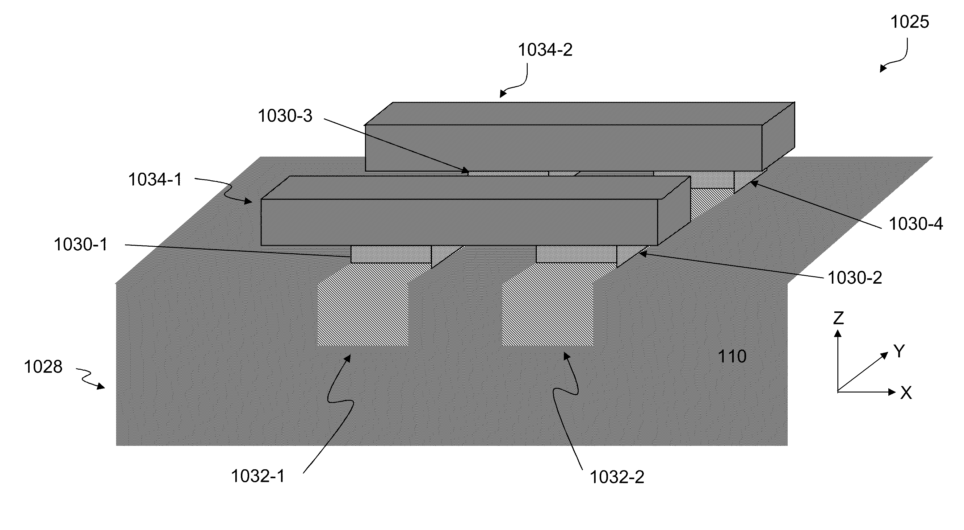
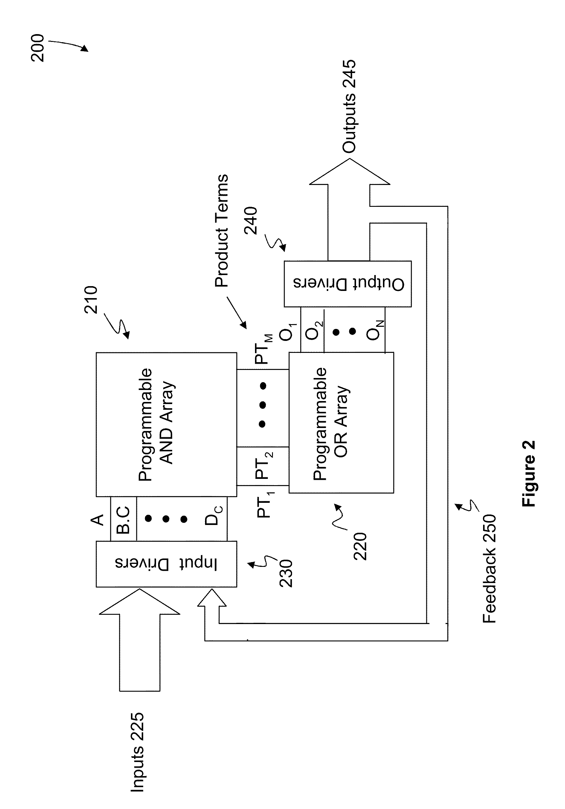
[0200]Integrated circuits for a wide variety of product applications in a competitive environment require fast time-to-market for new designs and low (or zero) non-recurring engineering cost (NRE) and low fabrication cost. As a result, the demand for field programmable devices (FPDs) solutions has increased rapidly. Low power is a requirement for most applications. Applications are increasingly portable so conservation of battery power is a requirement and nonvolatile operation is advantageous, especially since integration levels (more function) are increasing rapidly as is the requirement for high performance.

[0201]The present disclosure provides field programmable device (FPD) chips with large logic capacity and field programmability that are in-circuit programmable (in-place in the package without requiring sockets). They use small versatile nonvolatile nanotube switches that enable efficient architectures for dense low power and high performance chip implementations and are comp...


PUM


Abstract

Field programmable device (FPD) chips with large logic capacity and field programmability that are in-circuit programmable are described. FPDs use small versatile nonvolatile nanotube switches that enable efficient architectures for dense low power and high performance chip implementations and are compatible with low cost CMOS technologies and simple to integrate.

Description

CROSS REFERENCES TO RELATED APPLICATIONS [0001]This application claims priority under 25 U.S.C. §119(e) to U.S. Provisional Patent Application No. 61 / 088,828, filed Aug. 14, 2008, entitled “Nonvolatile Nanotube Programmable Logic Devices and a Nonvolatile Nanotube Field Programmable Gate Array Using Same.”[0002]This application is related to the following applications, the entire contents of which are incorporated herein by reference in their entirety:[0003]U.S. patent application Ser. No. TBA, filed concurrently herewith, entitled NONVOLATILE NANOTUBE PROGRAMMABLE LOGIC DEVICES AND A NONVOLATILE NANOTUBE FIELD PROGRAMMABLE GATE ARRAY USING SAME;[0004]U.S. patent application Ser. No. TBA, filed concurrently herewith, entitled NONVOLATILE NANOTUBE PROGRAMMABLE LOGIC DEVICES AND A NONVOLATILE NANOTUBE FIELD PROGRAMMABLE GATE ARRAY USING SAME;[0005]U.S. patent application Ser. No. TBA, filed concurrently herewith, entitled NONVOLATILE NANOTUBE PROGRAMMABLE LOGIC DEVICES AND A NONVOLATI...

Claims


Application Information

Patent Timeline
Patent Type & Authority Applications(United States)
IPC IPC(8): H01L29/66H01L27/088
CPCB82Y10/00G11C13/025G11C23/00G11C29/02G11C29/021G11C29/023Y10S977/94H03K19/17728H03K19/17736H03K19/1776H03K19/1778H03K19/17796G11C29/028G11C13/004G11C13/0061G11C13/0069G11C2013/0042G11C2013/0054G11C2213/82G11C13/0004G11C13/0007G11C2213/35
Inventor BERTIN, CLAUDE L.
Owner NANTERO
Why Eureka
Try Eureka