Soi substrates and devices on soi substrates having a silicon nitride diffusion inhibition layer and methods for fabricating

a technology of diffusion inhibition layer and silicon nitride, which is applied in the direction of semiconductor devices, basic electric elements, electrical equipment, etc., can solve the problems of affecting device performance and thin silicon layer

Inactive Publication Date: 2010-02-18
GLOBALFOUNDRIES INC
View PDF8 Cites 17 Cited by
  • Summary
  • Abstract
  • Description
  • Claims
  • Application Information

AI Technical Summary

Problems solved by technology

However, this structure provides only a very shallow silicon layer in which to form source and drain regions.
Even a minimal decrease in dopant concentration res

Method used


Image

  • Soi substrates and devices on soi substrates having a silicon nitride diffusion inhibition layer and methods for fabricating
  • Soi substrates and devices on soi substrates having a silicon nitride diffusion inhibition layer and methods for fabricating
  • Soi substrates and devices on soi substrates having a silicon nitride diffusion inhibition layer and methods for fabricating

Examples


Embodiment Construction

[0014]The following detailed description of the invention is merely exemplary in nature and is not intended to limit the invention or the application and uses of the invention. Furthermore, there is no intention to be bound by any theory presented in the preceding background of the invention or the following detailed description of the invention.

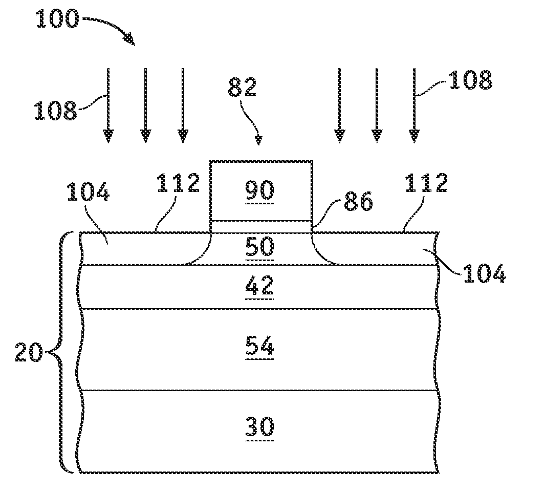
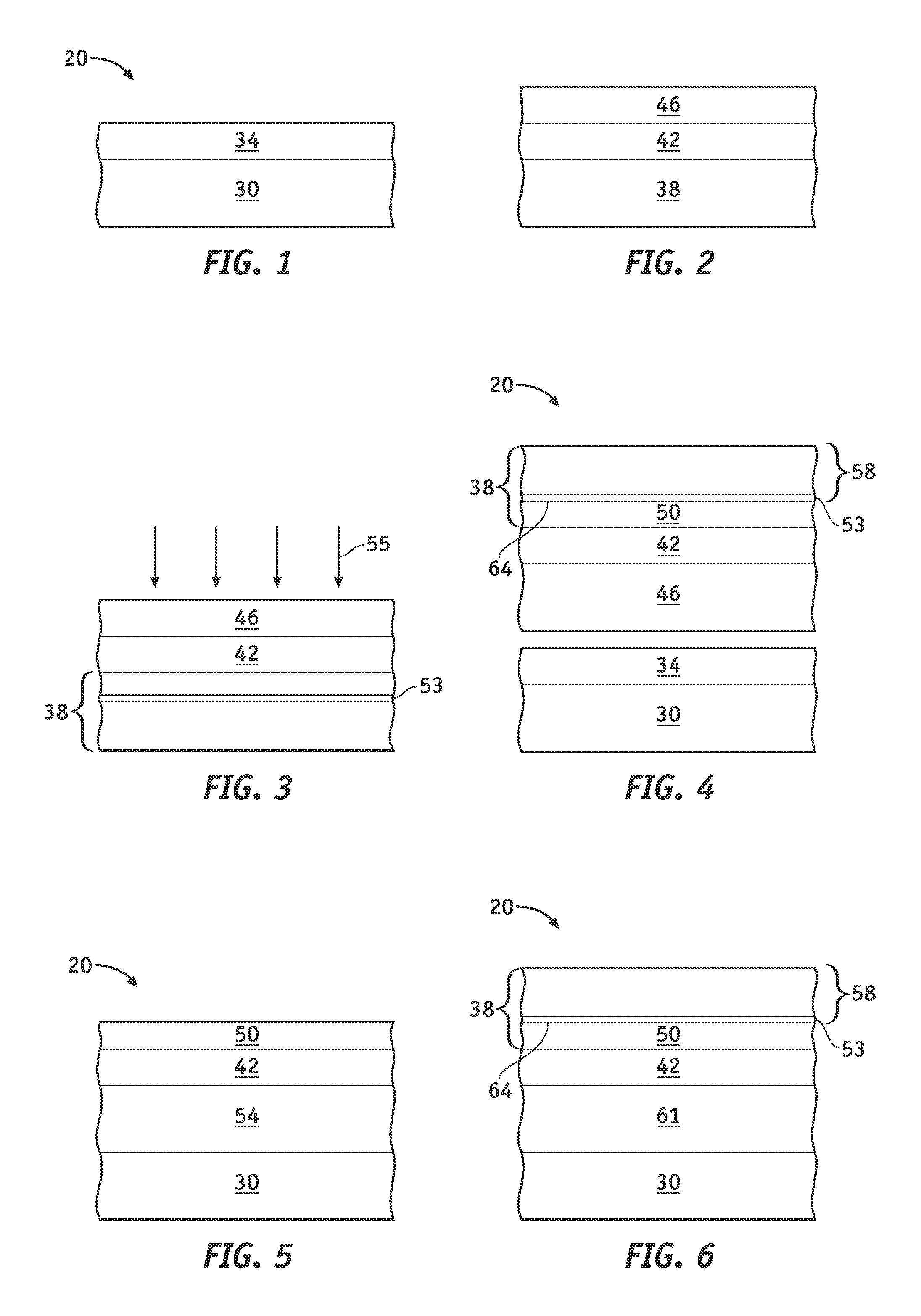
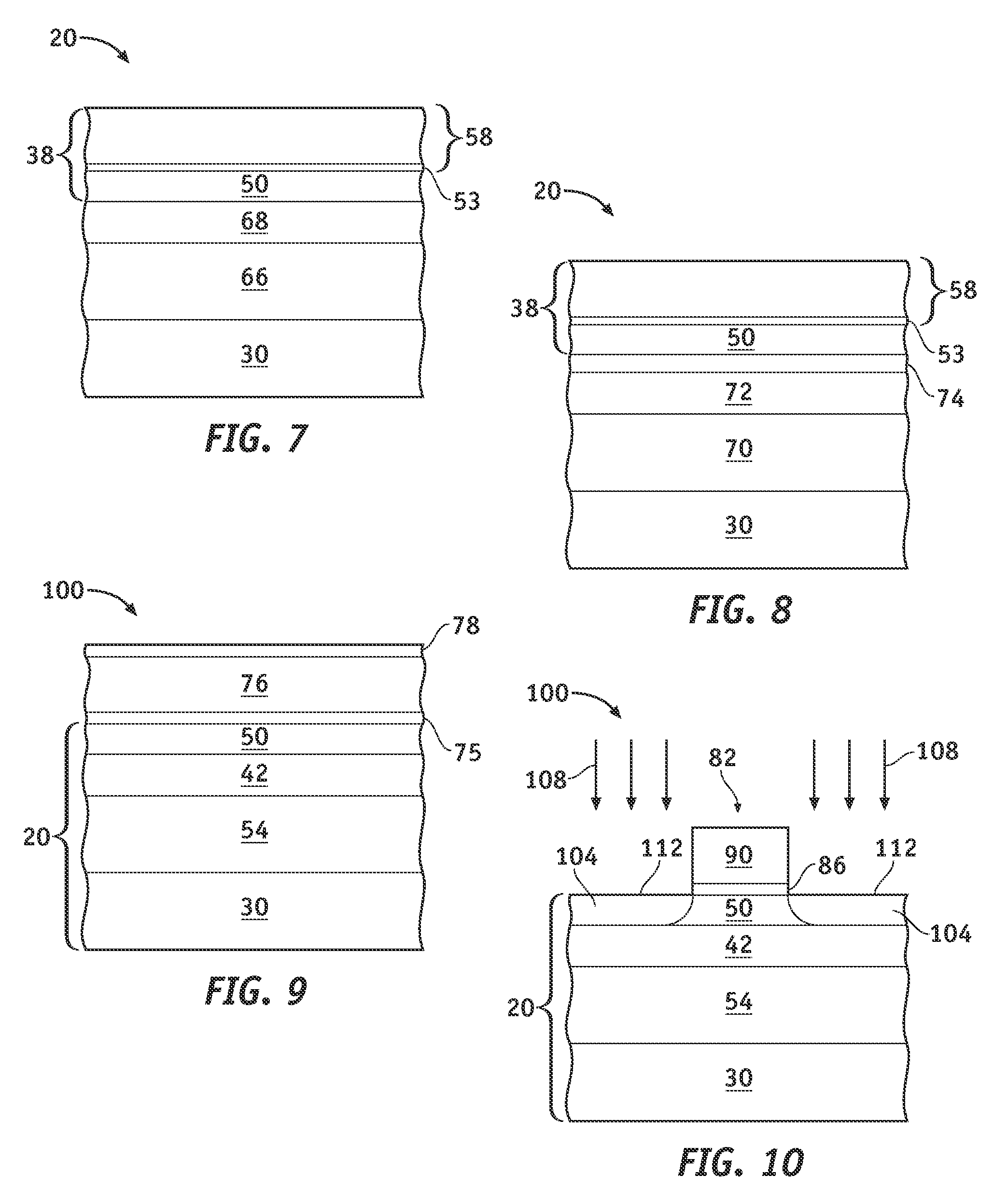
[0015]The various embodiments of the present invention result in the fabrication of an SOI substrate having a layer of silicon nitride interposed between a BOX layer and an uppermost, crystalline silicon layer of the SOI substrate. Various elements of a MOS transistor may be fabricated on and within this SOI substrate including gate stacks and source and drain regions. The nitride layer acts to inhibit the diffusion of source / drain impurity dopants such as boron or phosphorous into the BOX layer that may otherwise occur during subsequent high temperature processes such as annealing or thermal oxide growth. In this manner, the nitride layer h...


PUM


Abstract

Semiconductor-on-insulator substrates and methods for fabricating semiconductor-on-insulator substrates are provided. One exemplary method comprises providing a first silicon-comprising substrate, providing a second silicon-comprising substrate, forming a first silicon nitride layer overlying the second silicon-comprising substrate, and coupling the first silicon-comprising substrate to the second silicon-comprising substrate such that the first silicon nitride layer is interposed between the two substrates.

Description

TECHNICAL FIELD[0001]The present invention generally relates to semiconductor-on-insulator (SOI) substrates and devices fabricated on SOI substrates and methods for fabricating such substrates and devices, and more particularly relates to SOI substrates and devices fabricated on SOI substrates having a silicon nitride diffusion inhibition layer and methods for fabricating such SOI substrates and devices.BACKGROUND[0002]The majority of present day integrated circuits (ICs) are implemented by using a plurality of interconnected field effect transistors (FETs), also called metal oxide semiconductor field effect transistors (MOSFETs or MOS transistors). The ICs are usually formed using both P-channel FETs (PMOS transistors or PFETs) and N-channel FETs (NMOS transistors or NFETs) and the IC is then referred to as a complementary MOS or CMOS circuit. Certain improvements in performance of MOS ICs can be realized by forming the MOS transistors in a thin layer of semiconductor material over...

Claims


Application Information

Patent Timeline
IPC IPC(8): H01L21/762H01L29/78
CPCH01L21/76254H01L29/78603H01L29/66772
Inventor MAITRA, KINGSUKKERBER, ANDREAS
Owner GLOBALFOUNDRIES INC
Why Eureka
Try Eureka