Hdp-cvd process, filling-in process utilizing hdp-cvd, and hdp-cvd system

a technology of hdp-cvd and filling process, which is applied in the field of high densityplasma cvd (hdpcvd) process, can solve the problem of easy damage to the surface of the wafer, and achieve the effect of improving the quality of the material deposited

Active Publication Date: 2010-02-18
MACRONIX INT CO LTD
View PDF12 Cites 6 Cited by
  • Summary
  • Abstract
  • Description
  • Claims
  • Application Information

AI Technical Summary

Benefits of technology

[0006]Accordingly, this invention provides an HDP-CVD process that can improve the quality of the material deposited without damaging the wafer surface.
[0007]This invention also provides a filling-in process utilizing HDP-CVD, which can also improve the quality of the deposited material without damaging the wafer surface.
[0014]Since the wafer is pre-heated before being subjected to HDP-CVD, the film quality is improved. Meanwhile, since the wafer is pre-heated outside of the HDP-CVD chamber or is formed with a liner layer thereon before the pre-heating step conducted in the HDP-CVD chamber, device damage due to plasma ion bombardment is prevented. Moreover, in an embodiment where the wafer is pre-heated outside of the HDP-CVD chamber together with at least one other wafer, not only plasma damage is prevented in the pre-heating step of the HDP-CVD process, but also the time required for separately pre-heating the wafers in the HDP-CVD chamber in the prior art can be saved so that the wafer-per-hour (WPH) value is increased.

Problems solved by technology

However, since plasma is generated in the pre-heating step in the HDP-CVD chamber, the wafer surface is easily damaged by the ion bombardment from the plasma.

Method used


Image

  • Hdp-cvd process, filling-in process utilizing hdp-cvd, and hdp-cvd system
  • Hdp-cvd process, filling-in process utilizing hdp-cvd, and hdp-cvd system
  • Hdp-cvd process, filling-in process utilizing hdp-cvd, and hdp-cvd system

Examples


first embodiment

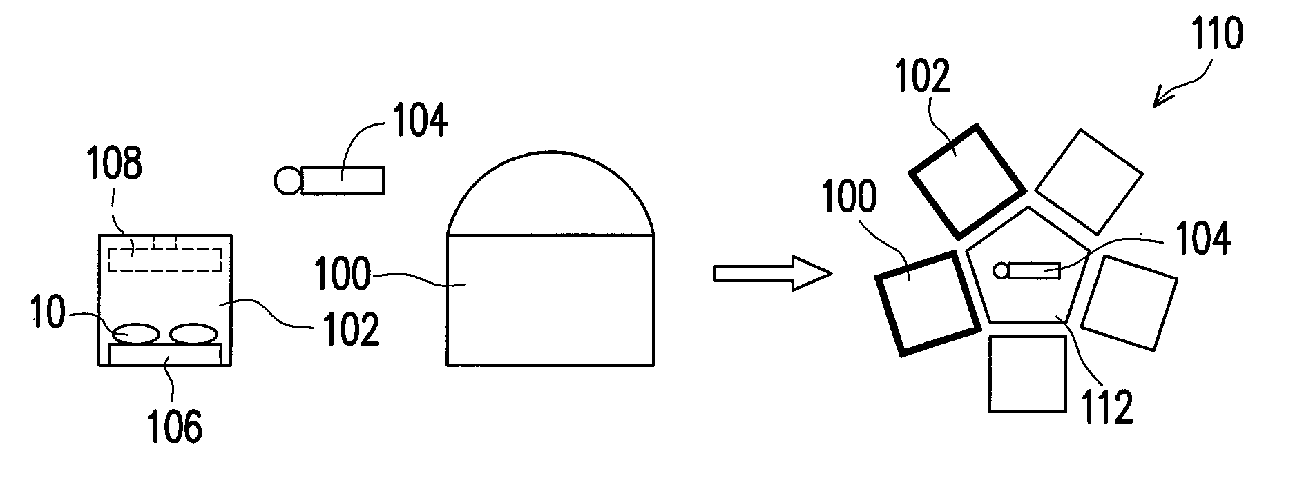
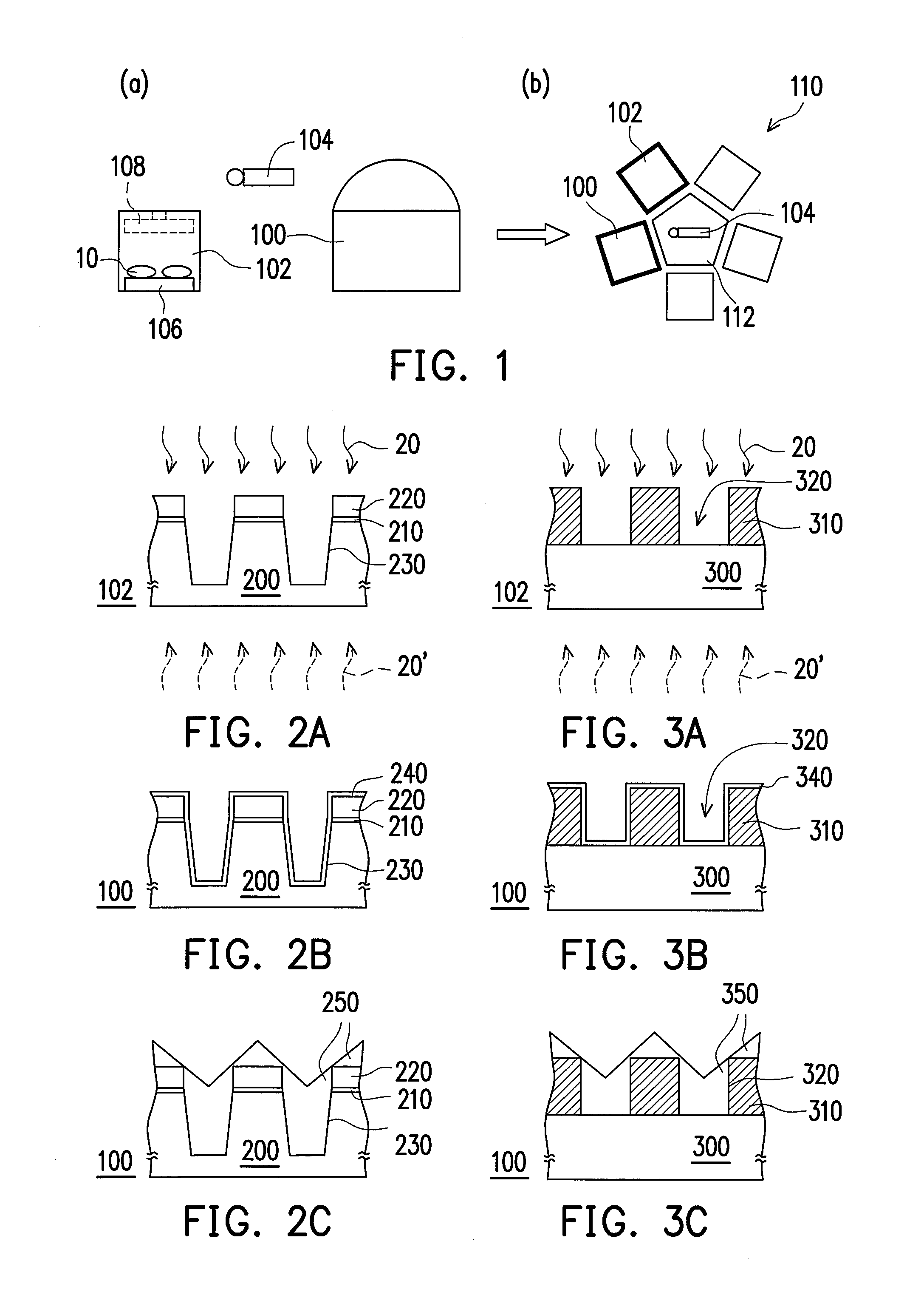
[0022]FIG. 1(a) illustrates an HDP-CVD system according to this invention and FIG. 1(b) a cluster tool incorporating the HDP-CVD system.

[0023]Referring to FIG. 1(a), the HDP-CVD system includes an HDP-CVD chamber 100 for conducting a deposition step that deposits a material, such as an insulating material like silicon oxide, on a wafer, a pre-heating chamber 102 as pre-heating means for conducting a pre-heating step outside of the HDP-CVD chamber 100, and wafer transfer means 104. The pre-heating chamber 102 is for pre-heating the wafer, before the wafer is loaded into the HDP-CVD chamber 100, to a temperature higher than room temperature and required in the deposition step to be conducted in the chamber 100.

[0024]The pre-heating chamber 102 may be equipped with a heating plate 106 or a heating lamp 108 for pre-heating the wafer, and may have a capacity of only one wafer 10 or a capacity allowing two or more wafers 10 of the same lot to be pre-heated therein simultaneously. For exam...

second embodiment

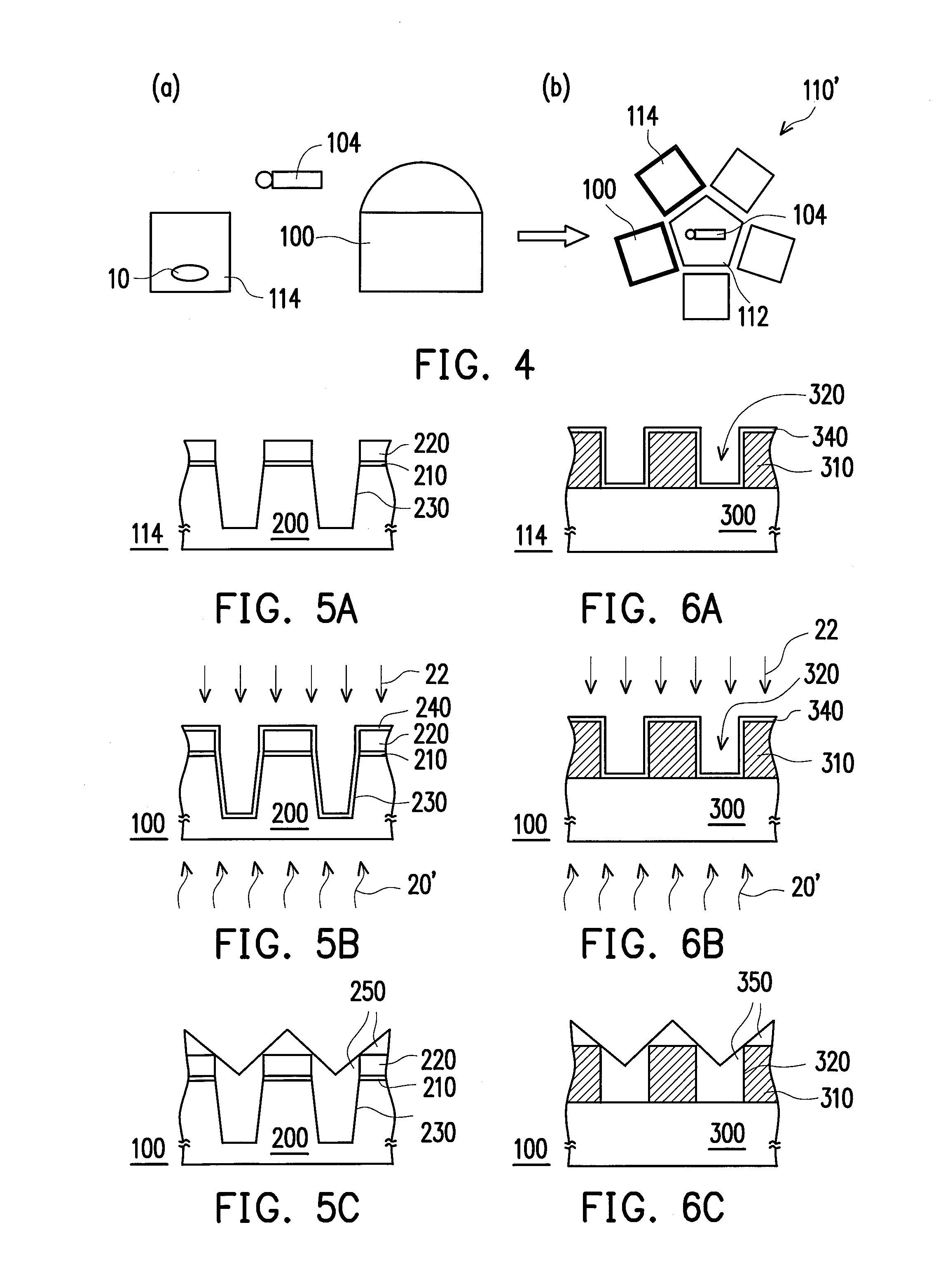
[0035]FIG. 4(a) illustrates a system for conducting a filling-in process according to this invention and FIG. 4(b) a cluster tool including the system.

[0036]Referring to FIG. 4(a), the system includes an HDP-CVD chamber 100 for conducting a pre-heating step and a deposition step, a chamber 114 for forming a liner layer on a wafer 10 before the pre-heating step, and wafer transfer means 104. In this embodiment, the HDP-CVD chamber 100 is set to pre-heat the wafer 10 to a temperature required in the deposition step to be conducted therein.

[0037]When the material to be deposited with HDP-CVD is silicon oxide, the chamber 114 may be one capable of depositing high-temperature oxide (HTO) or one capable of depositing silicon oxide through plasma-enhanced chemical vapor deposition (PECVD). The HTO may be formed through low-pressure chemical vapor deposition (LPCVD). As in the first embodiment, the wafer transfer means 104 is usually a robot.

[0038]Referring to FIG. 4(b), the HDP-CVD chamber...


PUM

PropertyMeasurementUnit
temperatureaaaaaaaaaa

Abstract

An HDP-CVD process is described, including a deposition step conducted in an HDP-CVD chamber and a pre-heating step that is performed outside of the HDP-CVD chamber before the deposition step and pre-heats a wafer to a temperature higher than room temperature and required in the HDP-CVD process deposition step.

Description

BACKGROUND OF THE INVENTION[0001]1. Field of Invention[0002]This invention relates to a semiconductor process, and more particularly relates to a high-density-plasma CVD (HDP-CVD) process, to a filling-in process utilizing HDP-CVD, and to an HDP-CVD system applicable to the HDP-CVD process.[0003]2. Description of Related Art[0004]As the linewidth of integrated circuit (IC) fabricating process is much reduced, the HDP-CVD technique is widely used in depositions of various materials, especially insulating materials, due to its gap-filling capability. An HDP-CVD process has both a deposition effect and an etching effect, wherein the etching effect is largest at the gap corners so that the material is well filled in the gaps.[0005]Moreover, to improve the quality of the deposited film, a wafer is usually pre-heated in-situ in the HDP-CVD chamber before the deposition is started. However, since plasma is generated in the pre-heating step in the HDP-CVD chamber, the wafer surface is easil...

Claims


Application Information

Patent Timeline
Patent Type & Authority Applications(United States)
IPC IPC(8): H01L21/31C23C16/00
CPCC23C16/0209C23C16/045C23C16/401H01L21/76224H01L21/02274H01L21/02304H01L21/31608H01L21/02164
Inventor LUOH, TUUNGSU, CHIN-TAYANG, TA-HUNGCHEN, KUANG-CHAOLUO, SHING-ANN
Owner MACRONIX INT CO LTD
Why Eureka
Try Eureka