High aspect ratio trench structures with void-free fill material

Active Publication Date: 2010-02-25
SEMICON COMPONENTS IND LLC
View PDF12 Cites 55 Cited by
  • Summary
  • Abstract
  • Description
  • Claims
  • Application Information

AI Technical Summary

Benefits of technology

[0022]In accordance with yet another embodiment of the invention, a method for forming a trench gate field effect transistor includes forming a trench in a semiconductor region. A conductive electrode is formed in the trench. The conductive electrode is insulated from the semiconductor region by a dielectric layer, the step of forming a conductive electrode includes: forming a conductive liner lining the dielectric layer along opposite sidewalls of the trench

Problems solved by technology

As a result, conventional methods for forming trench str

Method used


Image

  • High aspect ratio trench structures with void-free fill material
  • High aspect ratio trench structures with void-free fill material
  • High aspect ratio trench structures with void-free fill material

Examples


Example

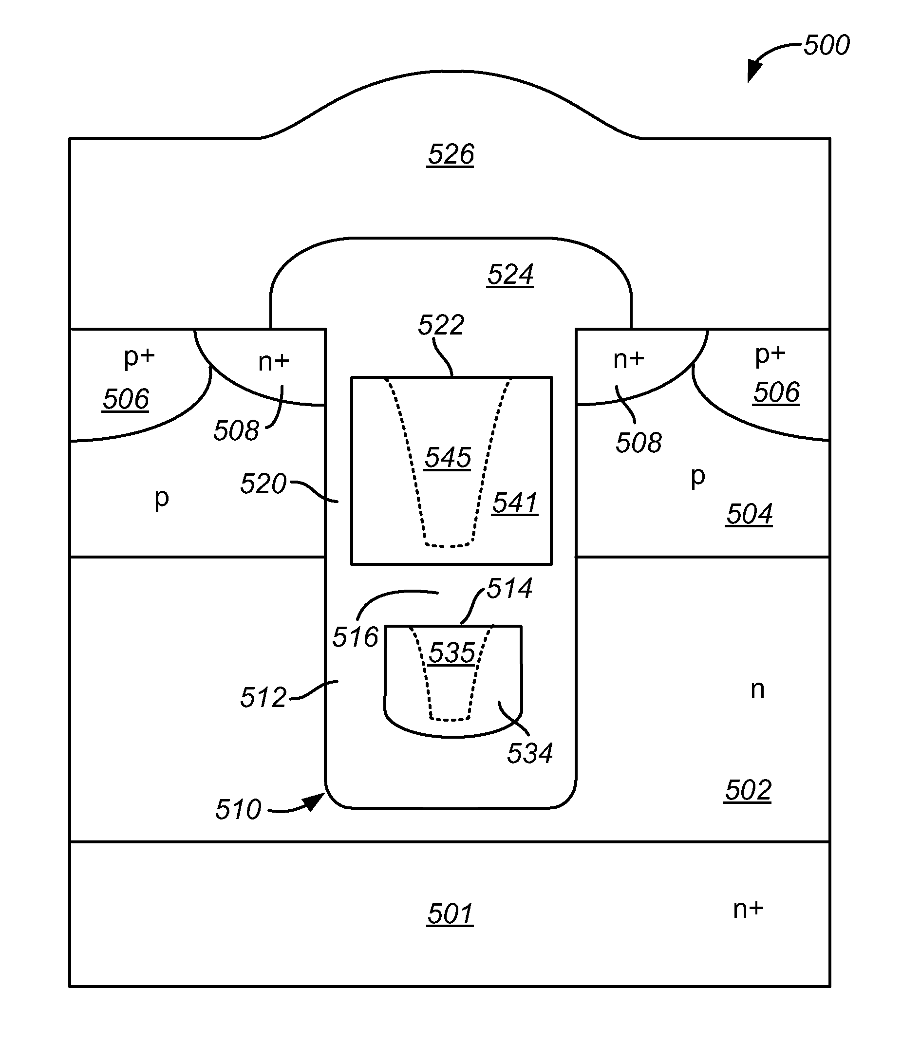
[0041]The present invention relates in general to semiconductor technology, and more particularly to structures and methods for forming high aspect ratio trenches and recesses. Merely by way of example, the invention has been applied to a method for void free filling of a trench with conductive materials in forming the shield electrode in shielded gate trench field effect transistors (FETs). In a specific embodiment, the trench is first partially filled with a first conductive material, which is etched back to provide a positive sidewall slope. A second conductive material is then used to fill the trench such that the trench is substantially void free. A method is also provided for filling a trench with reentrant sidewalls.

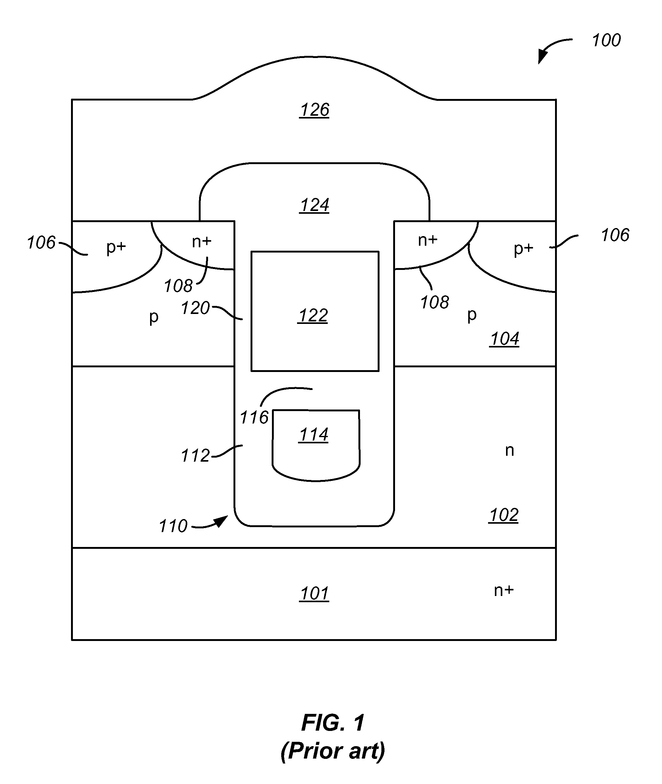
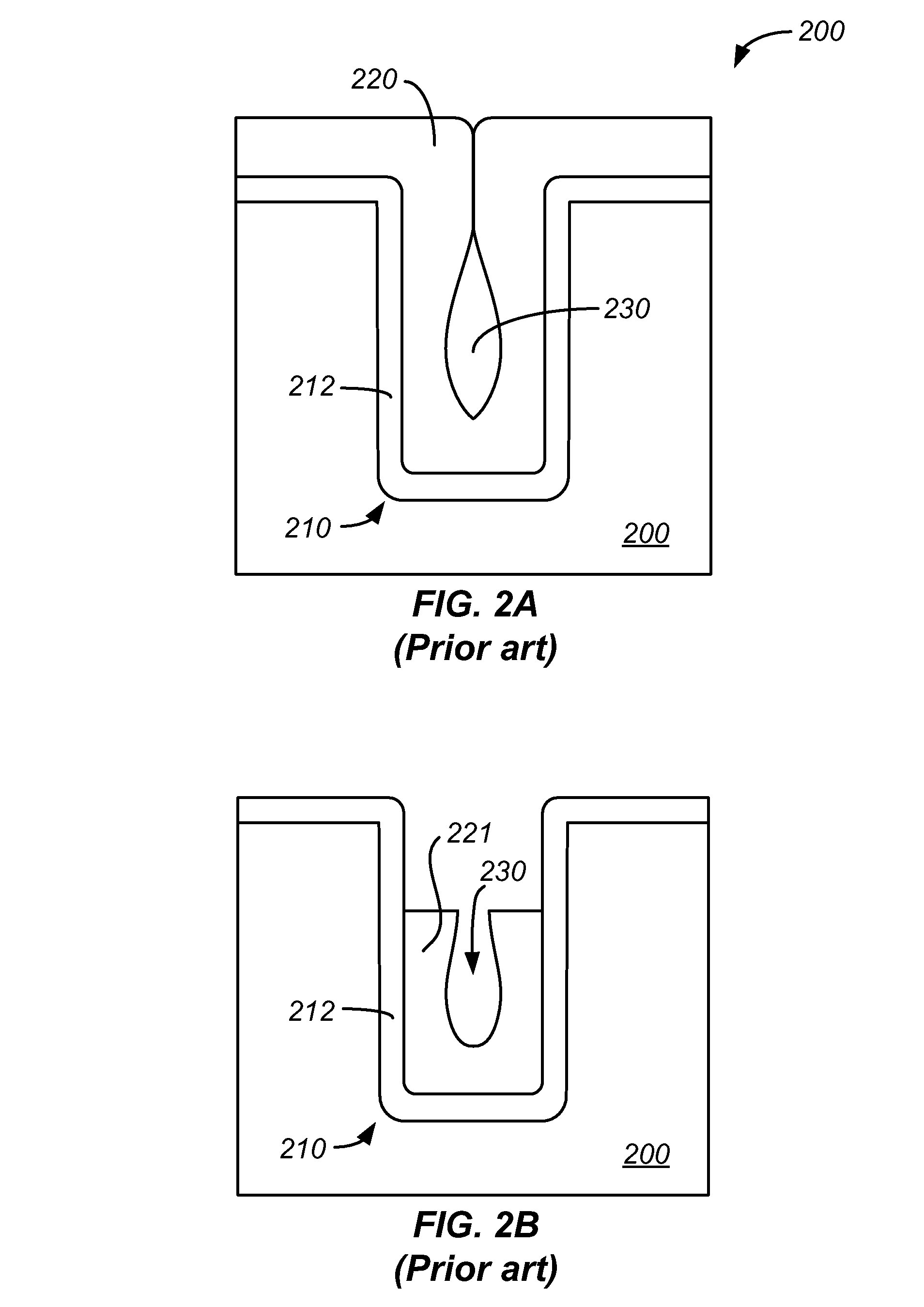
[0042]In forming a shielded gate FET, a conductive material is used to fill a trench and then etched back to thereby form a shield electrode in a bottom portion of the trench. FIG. 2A illustrates a conventional trench filling method. A trench 210 is formed in subs...


PUM


Abstract

A field effect transistor (FET) includes a trench extending into a semiconductor region. A conductive electrode is disposed in the trench, and the conductive electrode is insulated from the semiconductor region by a dielectric layer. The conductive electrode includes a conductive liner lining the dielectric layer along opposite sidewalls of the trench. The conductive liner has tapered edges such that a thickness of the conductive liner gradually increases from a top surface of the conductive electrode to a point in lower half of the conductive electrode. The conductive electrode further includes a conductive fill material sandwiched by the conductive liner. The FET further includes a drift region of a first conductivity type in the semiconductor region, and a body region of a second conductivity type extending over the drift region. Source regions of the first conductivity type extend in the body region adjacent the trench.

Description

CROSS-REFERENCES TO RELATED APPLICATIONS[0001]This application claims the benefit of U.S. Provisional Application No. 61 / 021,294, filed on Jan. 15, 2008, which is incorporated herein by reference in its entirety for all purposes.BACKGROUND OF THE INVENTION[0002]The present invention relates in general to semiconductor technology, and more particularly to structures and methods for forming high aspect ratio trenches. Merely by way of example, the invention has been applied in a shielded gate trench field effect transistor (FET). But it would be recognized that the invention has a much broader range of applicability.[0003]Shielded gate trench FETs and trench gate FETs are widely used in power electronics. In a shielded gate trench FET, the shield electrode reduces the gate-drain capacitance (Cgd) and improves the breakdown voltage of the transistor without sacrificing the transistor on-resistance. FIG. 1 is a simplified cross sectional view diagram of a conventional shielded gate tren...

Claims


Application Information

Patent Timeline
IPC IPC(8): H01L29/78H01L21/336
CPCH01L29/407H01L29/41766H01L29/4236H01L29/42368H01L29/456H01L29/7813H01L29/4933H01L29/495H01L29/4975H01L29/66727H01L29/66734H01L29/4925
Inventor MURPHY, JAMES J.CHEN, HUIVALDEZ, EILEEN
Owner SEMICON COMPONENTS IND LLC
Why Eureka
Try Eureka