

Silicon processing method and silicon substrate with etching mask
a silicon substrate and processing method technology, applied in the direction of microstructured devices, semiconductor/solid-state device testing/measurement, semiconductor/solid-state device details, etc., can solve the problems of spring constant error and manufacturing error of a resonant frequency of the micro oscillator, so as to reduce the spring constant error and the processing dimension error.
- Summary
- Abstract
- Description
- Claims
- Application Information
AI Technical Summary
Benefits of technology
Problems solved by technology
Method used
Image

Examples
first embodiment
[0041]A silicon processing method and a configuration example of a structure processed by the silicon processing method are described as a first embodiment of the present invention.
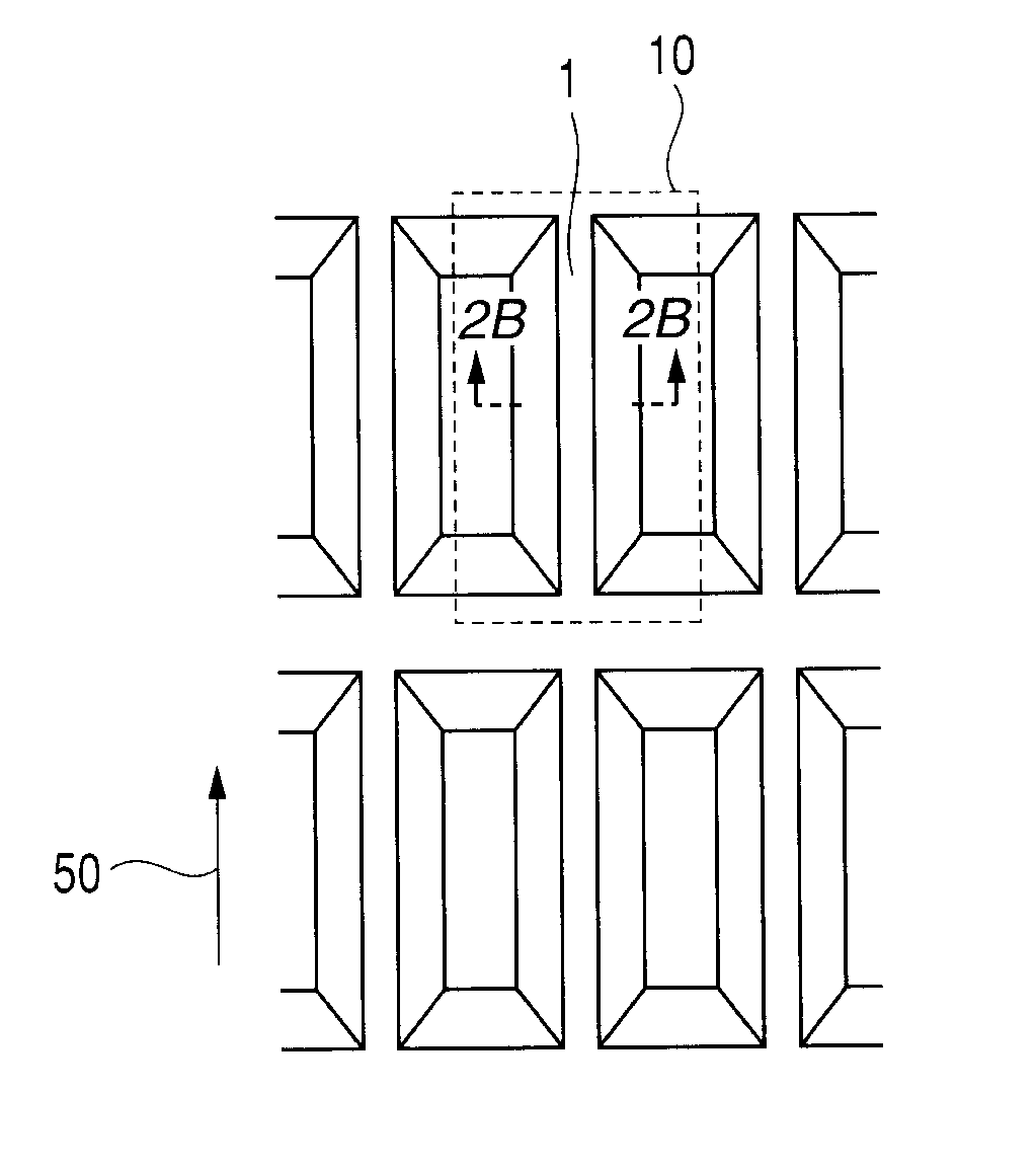
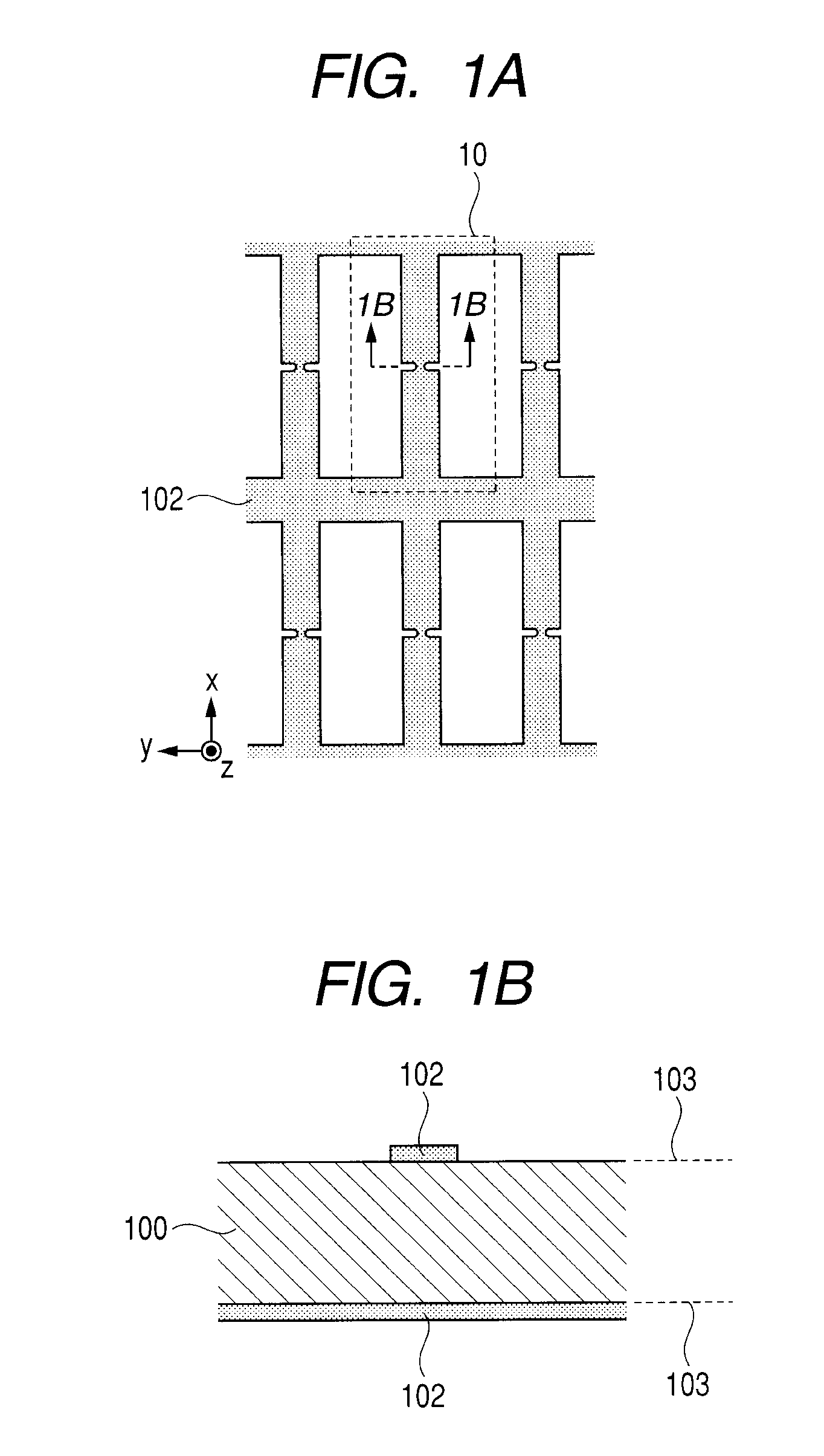
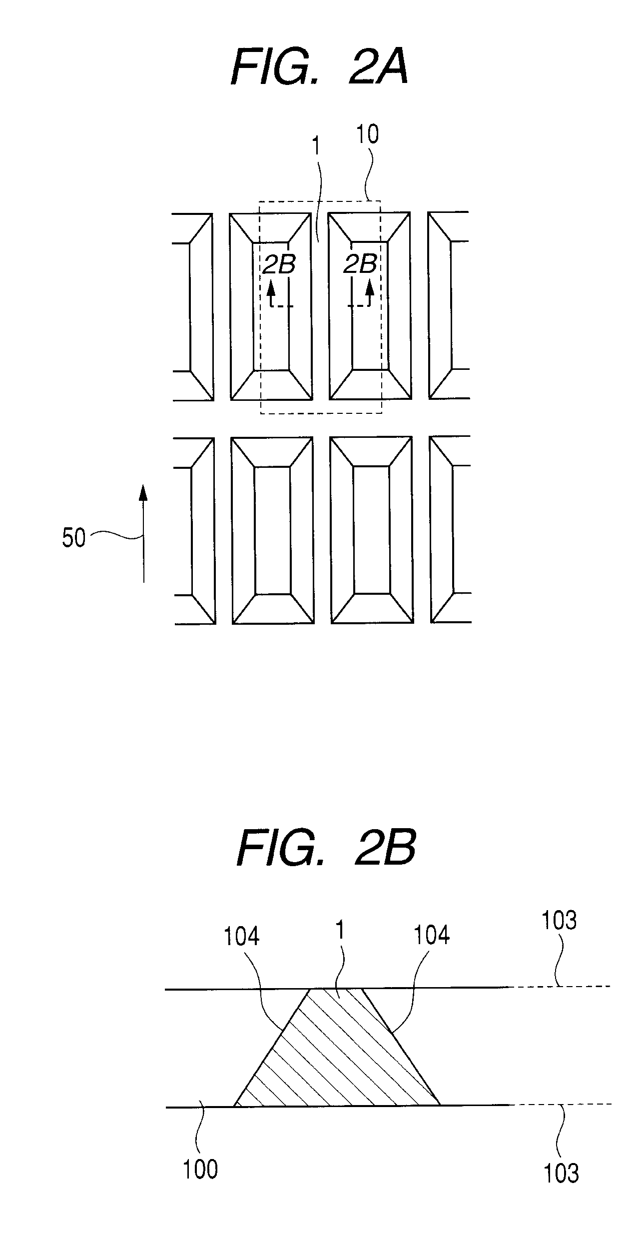
[0042]First, the silicon processing method according to this embodiment is described with reference to FIGS. 1A and 1B to FIG. 5. FIG. 5 is a top view of a silicon wafer 100 used for the silicon processing method according to this embodiment. The silicon wafer 100 is a single crystal of silicon. A normal direction on a paper surface of FIG. 5 is a crystal axis direction. The silicon wafer 100 has an orientation flat 105 indicating a crystal axis direction. An etching mask pattern 101 is formed on the surface of the silicon wafer 100. Plural structures can be formed by one wafer. Even if the etching mask pattern 101 has an alignment error with respect to the crystal axis direction, a processing dimension error of a structure to be formed can be reduced by the silicon processing method according to this ...
second embodiment
[0072]A second embodiment of the present invention is described. In FIGS. 11A to 11C, a configuration example of a micro oscillator manufactured by the silicon processing method according to this embodiment is illustrated. FIG. 11A is a top view of the micro oscillator and FIG. 11B is a sectional view taken along line 11B-11B of FIG. 11A. FIGS. 12A to 12C are diagrams illustrating a light deflector including the micro oscillator according to this embodiment. FIG. 12A is a top view of the light deflector and FIG. 12B is a sectional view taken along a line 12B-12B of FIG. 12A. In these figures, components having functions same as those in the first embodiment are denoted by the same reference numerals and signs.
[0073]In the micro oscillator illustrated in FIGS. 11A to 11C and the light deflector illustrated in FIGS. 12A to 12C, reference numeral 2 denotes a supporting section, 3 denotes a fixing section, 4 denotes a reflection surface, 6 denotes a movable section, 7 denotes a permanen...
third embodiment
[0089]A third embodiment of the present invention is described. FIG. 12C is a schematic perspective view illustrating an optical apparatus according to the third embodiment in which the light deflector illustrated in FIGS. 12A to 12C in the second embodiment is used.
[0090]An image forming apparatus is illustrated as the optical apparatus. In FIG. 12C, reference numeral 3003 denotes the light deflector according to the second embodiment, which one-dimensionally scans incident light. Reference numeral 3001 denotes a laser beam source as a light source. Reference numeral 3002 denotes a lens or a lens group, 3004 denotes a writing lens or a writing lens group, and 3005 denotes a drum-like photosensitive member as a light irradiation target.
[0091]A laser beam emitted from the laser beam source 3001 is subjected to predetermined intensity modulation related to timing for light deflection scanning. This intensity modulated light is one-dimensionally scanned by the optical scanning system (...
PUM
| Property | Measurement | Unit |
|---|---|---|
| width W1 | aaaaa | aaaaa |
| length L1 | aaaaa | aaaaa |
| width | aaaaa | aaaaa |
Abstract
Description
Claims
Application Information