
Semiconductor device and method of manufacturing the same

a semiconductor and device technology, applied in semiconductor devices, diodes, electrical apparatus, etc., can solve the problems of increasing processing time, complex processes, and reducing breakdown voltag

Active Publication Date: 2010-03-04
SEMICON COMPONENTS IND LLC
View PDF4 Cites 5 Cited by
  • Summary
  • Abstract
  • Description
  • Claims
  • Application Information

AI Technical Summary

Benefits of technology

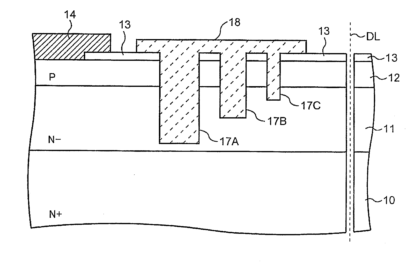
[0013]The invention also provides a method of manufacturing a semiconductor device. The method includes forming a semiconductor layer on a semiconductor substrate, forming an electronic device in the semiconductor layer, and forming a plurality of grooves in the semiconductor layer so as to surround the electronic device in plan view of the semiconductor device. The grooves have depths different from each other. The method further includes depositing an insulating material in each of the grooves to form a guard ring comprising the grooves having the insulating material therein, and dicing the semiconductor substrate and the semiconductor layer along a dicing line provided outside the guard ring.
[0069]Furthermore, since the repetition of the process of depositing the insulating material in the groove, that has been needed conventionally, is not necessary, the process of forming the guard ring or the element isolation layer as described above is simplified, and further the amount of the insulating material deposited in the grooves forming the guard ring or the like is minimized, compared with the conventional device. Furthermore, there is no need to consider the accuracy or stability when the insulating material is deposited in the grooves, unlike the conventional device. As a result, the manufacturing cost is prevented from increasing.
[0013]The invention also provides a method of manufacturing a semiconductor device. The method includes forming a semiconductor layer on a semiconductor substrate, forming an electronic device in the semiconductor layer, and forming a plurality of grooves in the semiconductor layer so as to surround the electronic device in plan view of the semiconductor device. The grooves have depths different from each other. The method further includes depositing an insulating material in each of the grooves to form a guard ring comprising the grooves having the insulating material therein, and dicing the semiconductor substrate and the semiconductor layer along a dicing line provided outside the guard ring.
[0071]Furthermore, in the case that the plurality of grooves is formed so as to gradually deepen toward the electronic device, when a reverse bias is applied, the innermost groove prevents the depletion layer from the semiconductor layer from reaching the damaged layer of the surface cut along the dicing lines. This prevents a leakage current between the semiconductor layer and the damaged layer.

Problems solved by technology

This causes a problem of reducing the breakdown voltage at the PN junction portion in the mesa groove 117 that functions as the guard ring.
However, this method causes complex processes and increases the processing time, and also makes it difficult to form the insulating material 118 stably with desired accuracy.
Furthermore, it causes a problem of largely increasing the amount of the insulating material 118 deposited in the mesa groove 117 more than the amount usually needed.
As a result, the manufacturing cost of the mesa diode is increased.

Method used


Image

  • Semiconductor device and method of manufacturing the same
  • Semiconductor device and method of manufacturing the same
  • Semiconductor device and method of manufacturing the same

Examples


first embodiment

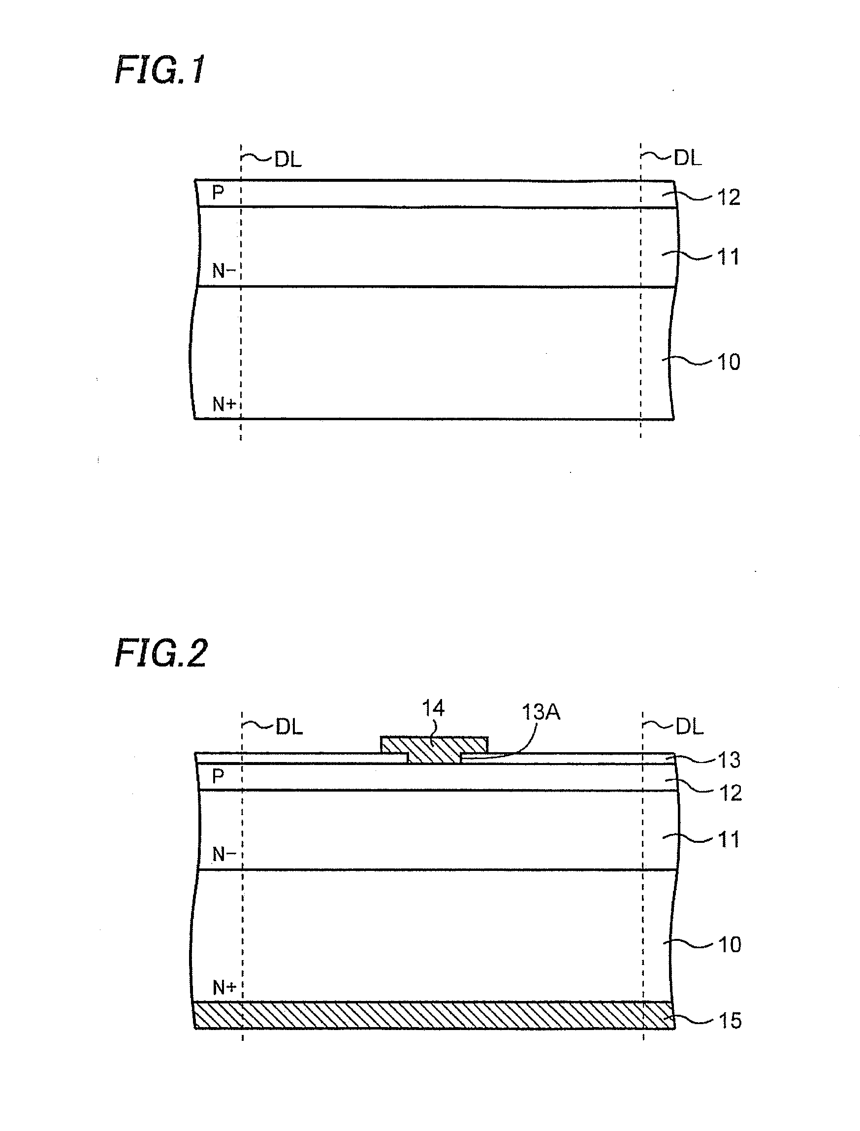
[0021]A semiconductor device and a method of manufacturing the same of the invention will be described. This embodiment uses a mesa diode as an example. FIGS. 1, 2, 4 and 6 are cross-sectional views showing the mesa diode and the method of manufacturing the same of the embodiment. FIGS. 1 and 2 mainly show a semiconductor wafer in a region for forming one of a plurality of mesa diodes to be formed thereon. FIGS. 4 and 6 show a partially enlarged view of FIGS. 1 and 2 near a dicing line DL.

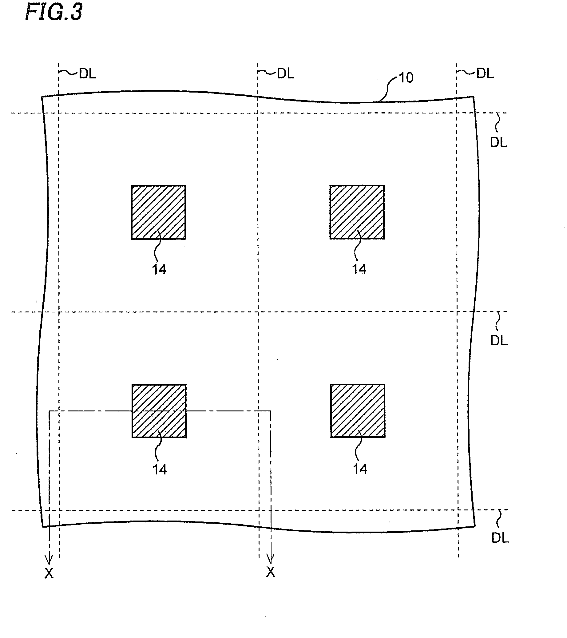
[0022]Furthermore, FIGS. 3 and 5 are plan views showing the mesa diode and the method of manufacturing the same of the embodiment of the invention, and show a portion of a region for forming the plurality of mesa diodes. A cross-section of FIG. 3 along line X-X corresponds to the cross-sectional views of FIGS. 1 and 2, and a cross-section of FIG. 5 along line Y-Y corresponds to the cross-sectional views of FIGS. 4 and 6.

[0023]As shown in FIG. 1, an N+ type semiconductor substrate 10 made of, for ex...

second embodiment

[0050]The plurality of grooves forming the guard ring of the embodiment, i.e., the first groove 17A, the second groove 17B and the third groove 17C may be positioned in the reverse depth order to the above. This case will be described as the invention referring to FIG. 7. FIG. 7 is a cross-sectional view showing a mesa diode and a method of manufacturing the same of the embodiment, and shows the same region as that of FIG. 6.

[0051]In this embodiment, among the first groove 17A, the second groove 17B and the third groove 17C, one of the two grooves next to each other, that is closer to the anode electrode 14, is formed deeper than the other on the outside of the one. In detail, the first groove 17A is deeper than the second groove 17B, and the second groove 17B is deeper than the third groove 17C. The number of the grooves may be different from the above, and the relation among the depths of the grooves in this case is the same as the above. In the same manner to the first embodiment...


PUM


Abstract

The invention is directed to reduction of a manufacturing cost and enhancement of a breakdown voltage of a PN junction portion abutting on a guard ring. An N− type semiconductor layer is formed on a front surface of a semiconductor substrate, and a P type semiconductor layer is formed thereon. An insulation film is formed on the P type semiconductor layer. Then, a plurality of grooves, i.e., a first groove, a second groove and a third groove are formed from the insulation film to the middle of the N− type semiconductor layer in the thickness direction thereof. The plurality of grooves is formed so that one of the two grooves next to each other among these, that is closer to an electronic device, i.e., to an anode electrode, is formed shallower than the other located on the outside of the one. Then, an insulating material is deposited in the first groove, the second groove and the third groove. The lamination body of the semiconductor substrate and the layers laminated thereon is then diced along dicing lines.

Description

CROSS-REFERENCE OF THE INVENTION[0001]This application claims priority from Japanese Patent Application No. 2008-227180, the content of which is incorporated herein by reference in its entirety.BACKGROUND OF THE INVENTION[0002]1. Field of the Invention[0003]The invention relates to a semiconductor device and a method of manufacturing the same.[0004]2. Description of the Related Art[0005]A high-power mesa diode has been conventionally known as one of semiconductor devices. A conventional mesa diode will be described referring to FIG. 8.[0006]An N− type semiconductor layer 111 is formed on the front surface of an N+ type semiconductor substrate 110. A P type semiconductor layer 112 is formed on the front surface of the N− type semiconductor layer 111, and an insulation film 113 is formed on the P type semiconductor layer 112. An anode electrode 114 electrically connected to the P type semiconductor layer 112 is further formed.[0007]A mesa groove 117 is formed from the front surface of...

Claims


Application Information

Patent Timeline
Patent Type & Authority Applications(United States)
IPC IPC(8): H01L29/06H01L21/762
CPCH01L21/76229H01L29/8611H01L29/7322H01L29/0615H01L23/3178H01L29/86
Inventor SUZUKITSUCHIYA, NAOFUMIKAMEYAMA, KOUJIRO
Owner SEMICON COMPONENTS IND LLC
Learn More