Light Emitting Element, Light Emitting Device, and Electronic Device

a technology light emitting devices, which is applied in the direction of discharge tubes/lamp details, discharge tubes luminescnet screens, electric discharge lamps, etc., can solve the problems of difficult to obtain point sources, and the inability to transfer the triplet excitation energy of blue emissive fluorescent compounds to an anode side, etc., to achieve the reduction of power consumption of light emitting elements, light emitting devices, and electronic devices.

Active Publication Date: 2010-03-04
SEMICON ENERGY LAB CO LTD
View PDF35 Cites 142 Cited by
  • Summary
  • Abstract
  • Description
  • Claims
  • Application Information

AI Technical Summary

Benefits of technology

[0029]By application of an embodiment of the present invention, the singlet exciton and the triplet exciton which are generated in the light emitting layer can be effectively used, and a light emitting element with high luminous efficiency can be realized.
[0030]In addition, by application of an embodiment of the present invention, power consumption of a light emitting element, a light emitting device, and an electronic device can be reduced.

Problems solved by technology

This is a feature that is hard to be obtained in point sources typified by an incandescent lamp and an LED or linear sources typified by a fluorescent light.
On the other hand, since an electron blocking layer (EBL) having greater triplet-excitation energy than that in the Blue LEL is provided on the anode side of the Blue LEL, the transfer of the triplet excitation energy of the blue emissive fluorescent compound to an anode side is impossible.

Method used


Image

  • Light Emitting Element, Light Emitting Device, and Electronic Device
  • Light Emitting Element, Light Emitting Device, and Electronic Device
  • Light Emitting Element, Light Emitting Device, and Electronic Device

Examples


embodiment 1

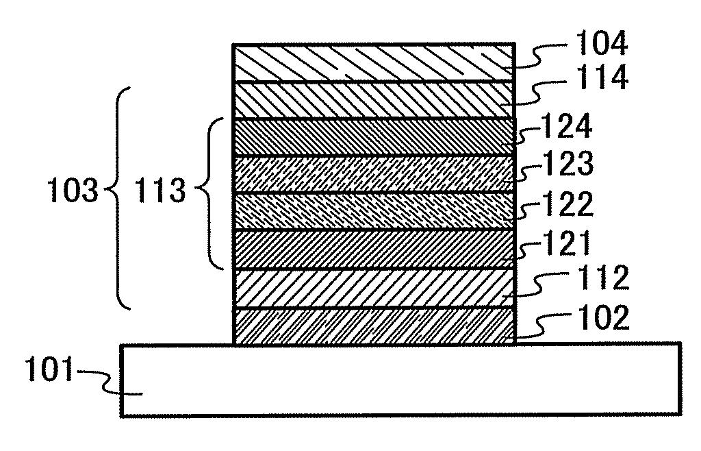
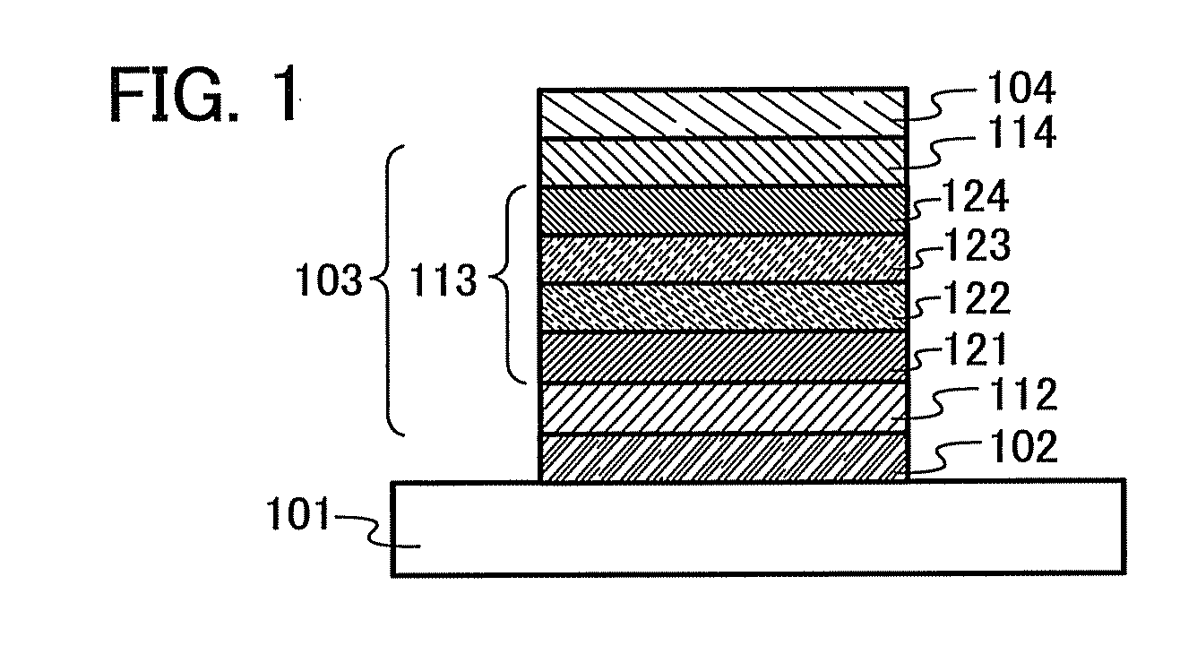
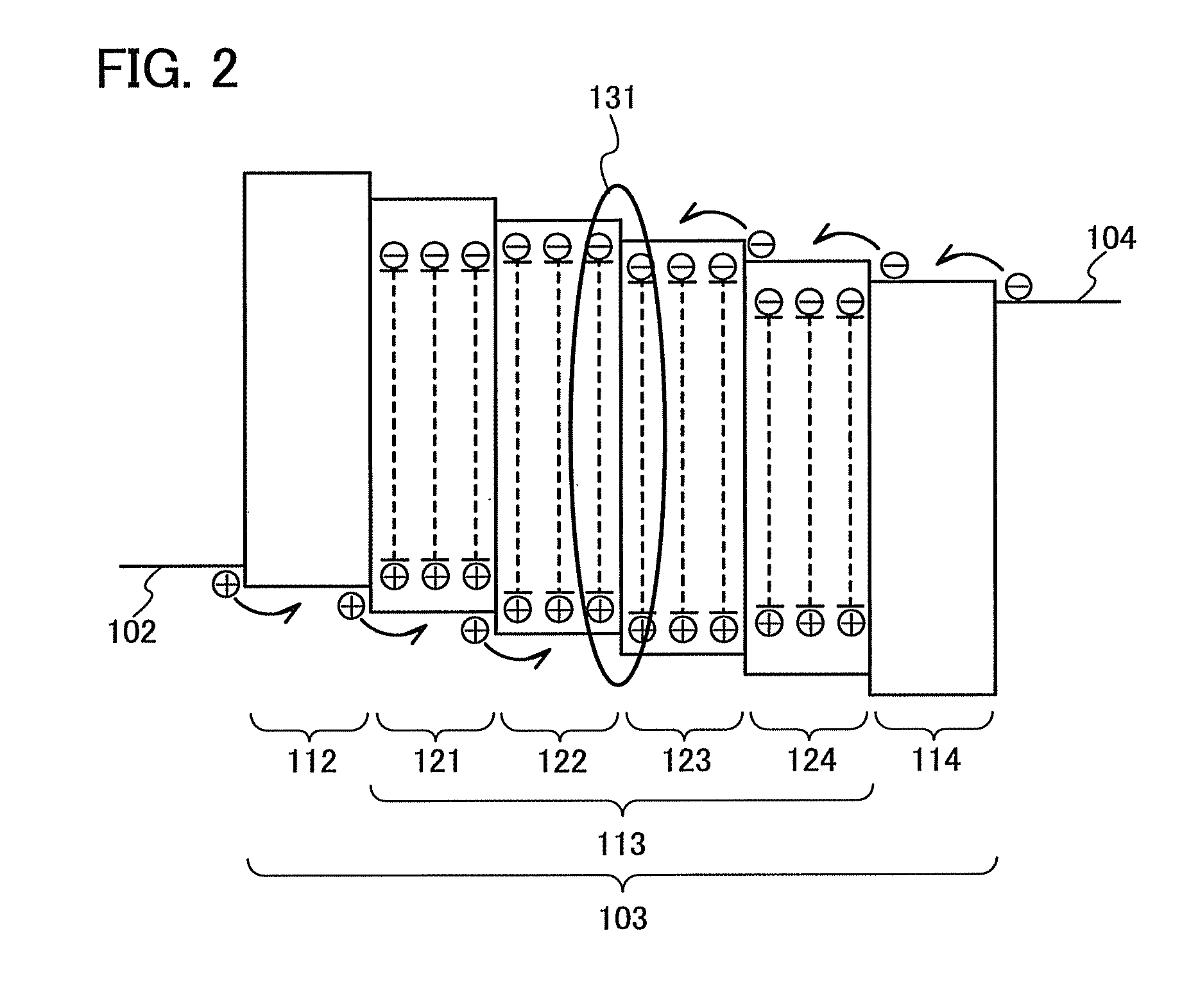
[0048]A mode of a light emitting element according to an embodiment of the present invention is described with reference to FIGS. 1, 2, 3, and 4.

[0049]The light emitting element according to an embodiment of the present invention has a plurality of layers between a pair of electrodes. In this specification, the plurality of layers formed between the pair of electrodes is collectively referred to as an EL layer. The EL layer has at least a light emitting layer.

[0050]In this embodiment, the light emitting element includes a first electrode 102, a second electrode 104, and an EL layer 103 formed between the first electrode 102 and the second electrode 104, as illustrated in FIG. 1. Note that in this embodiment, the first electrode 102 serves as an anode and the second electrode 104 serves as a cathode. In other words, when voltage is applied to the first electrode 102 and the second electrode 104 such that potential of the first electrode 102 is higher than that of the second electrode...

embodiment 2

[0111]In this embodiment, a light emitting element (a stacked type element) in which a plurality of light emitting units according to an embodiment of the present invention is stacked will be described with reference to FIG. 7. This light emitting element is a light emitting element having a plurality of light emitting units between a first electrode and a second electrode. As the light emitting units, at least a light emitting layer may be included, and a structure similar to that of the EL layer described in Embodiment 1 can be used. In other words, the light emitting element described in Embodiment 1 is a light emitting element having one light emitting unit, and a light emitting element having a plurality of light emitting units will be described in this embodiment.

[0112]In FIG. 7, a first light emitting unit 511 and a second light emitting unit 512 are stacked between a first electrode 501 and a second electrode 502. A charge generation layer 513 is provided between the first l...

embodiment 3

[0118]In this embodiment, a light emitting device having a light emitting element according to an embodiment of the present invention will be described.

[0119]A light emitting device having the light emitting element according to an embodiment of the prevent invention in a pixel portion will be described in this embodiment with reference to FIGS. 8A and 8B. FIG. 8A is a top view illustrating the light emitting device, and FIG. 8B is a cross sectional view taken along line A-A′ and line B-B′ of FIG. 8A. This light emitting device includes a driver circuit portion (source side driver circuit) 601, a pixel portion 602, and a driver circuit portion (gate side driver circuit) 603 which are illustrated by dotted lines in order to control the light emission of the light emitting element. Reference numeral 604 denotes a sealing substrate; reference numeral 605 denotes a sealing material; and a portion surrounded by the sealing material 605 corresponds to a space 607.

[0120]Note that a leading...


PUM


Abstract

An object is to improve luminous efficiency of a light emitting element using triplet exciton energy effectively. Another object is to reduce power consumption of a light emitting element, a light emitting device, and an electronic device. Triplet exciton energy generated in a light emitting layer which exhibits short wavelength fluorescence can be effectively utilized by use of a structure in which the light emitting layers which exhibit short wavelength fluorescence are sandwiched between light emitting layers each including a phosphorescent compound. Further, the emission balance can be improved between the light emitting layer including a phosphorescent compound and the light emitting layer which exhibits fluorescence by the devising of the structure of the light emitting layer which exhibits fluorescence.

Description

BACKGROUND OF THE INVENTION[0001]1. Field of the Invention[0002]The present invention relates to light emitting elements using electroluminescence. In addition, the present invention relates to a light emitting device and an electronic device having the light emitting element.[0003]2. Description of the Related Art[0004]In recent years, research and development has been extensively conducted on light emitting elements using electroluminescence. In a basic structure of these light emitting elements, a substance having a light emitting property is interposed between a pair of electrodes. By application of voltage to these elements, light emission can be obtained from the substance having a light emitting property.[0005]Since such a light emitting element is of self-light emitting type, it is considered that the light emitting element has advantages over a liquid crystal display in that visibility of pixels is high, backlight is not required, and the like and is therefore suitable for ...

Claims


Application Information

Patent Timeline
Patent Type & Authority Applications(United States)
IPC IPC(8): H01L51/50
CPCH01L51/5016H01L51/5036H01L51/5048H01L51/5278H01L33/26H01L51/5088H01L51/50H01L51/00H01L51/504H01L51/5024H01L51/5012H10K50/11H10K2101/10H10K50/125H10K50/13H10K50/14H10K50/19H10K50/12H10K50/17H10K50/00H10K2102/351H10K99/00
Inventor IKEDA, KAORUSEO, SATOSHI
Owner SEMICON ENERGY LAB CO LTD
Why Eureka
Try Eureka