Static random access memory (SRAM) and test method of the SRAM having precharge circuit to precharge bit line

a random access memory and test method technology, applied in static storage, information storage, digital storage, etc., can solve the problems of abnormality of memory cells, small static noise margin of memory cells, and high fraction defective, so as to improve the detection sensitivity of abnormal memory cells, and control the increase in the circuit area of sram

Active Publication Date: 2010-03-04
RENESAS ELECTRONICS CORP
View PDF2 Cites 8 Cited by
  • Summary
  • Abstract
  • Description
  • Claims
  • Application Information

AI Technical Summary

Benefits of technology

[0024]According to the exemplary aspect, it is possible to improve the detection sensitivity of the abnormal memory cell whose SNM is small while controlling increase in the circuit area of the SRAM.

Problems solved by technology

There is a case where even when a read test is performed on the SRAM of this configuration, the memory cell that has a small Static Noise Margin (SNM) and a high fraction defective cannot be detected.
As in the above, there is a case where even when the SNM is inspected by the read test by the related technology, the abnormality of the memory cell cannot be detected.

Method used


Image

  • Static random access memory (SRAM) and test method of the SRAM having precharge circuit to precharge bit line
  • Static random access memory (SRAM) and test method of the SRAM having precharge circuit to precharge bit line
  • Static random access memory (SRAM) and test method of the SRAM having precharge circuit to precharge bit line

Examples


first exemplary embodiment

1. First Exemplary Embodiment

[0040]A first exemplary embodiment of SRAM and a read test method of the SRAM according to the present invention will be described with reference to FIG. 5 and FIG. 6.

(Configuration of SRAM)

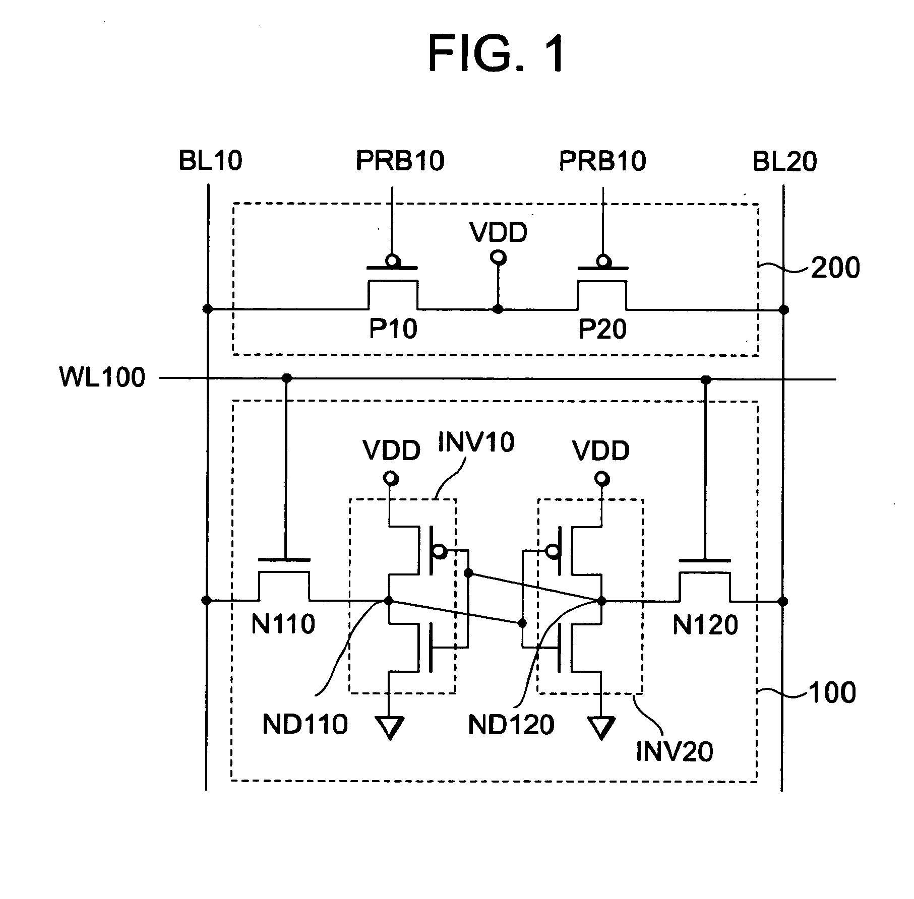
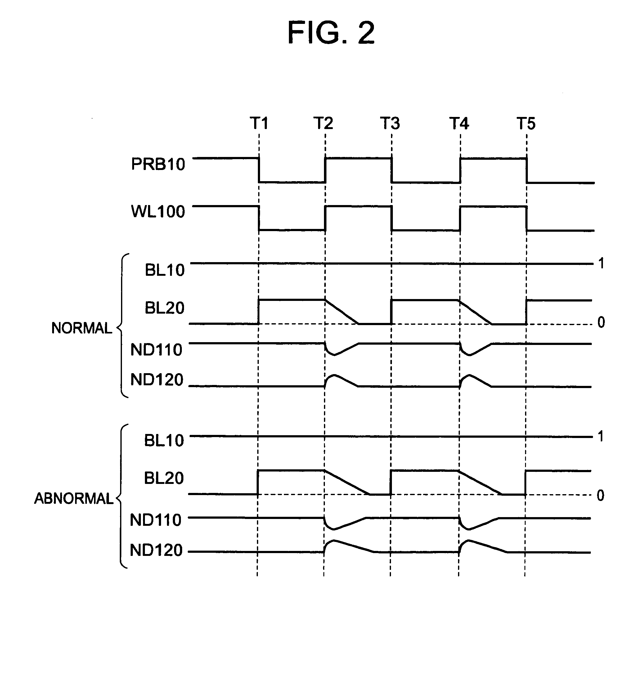
[0041]FIG. 5 is a diagram showing a part of a configuration of the SRAM in the first exemplary embodiment. The SRAM includes a memory cell 10 connected to the bit line pair BL1, BL2 and the word line WL10, a precharge circuit 20 for precharging the bit line pair BL1, BL2, and a precharge control circuit 30 for controlling the precharge circuit 20. The precharge control circuit 30 also controls the precharge circuit connected to an other bit line pair being not illustrated.

[0042]Referring to FIG. 5, the memory cell 10 include a positive feedback loop (a flip-flop) that includes two CMOS inverters INV1, INV2 and, two N-channel MOS transistors N11, N12 (hereinafter referred to as selection transistors N11, N12) for controlling a connection between the bit line pair BL1, ...

second exemplary embodiment

2. Second Exemplary Embodiment

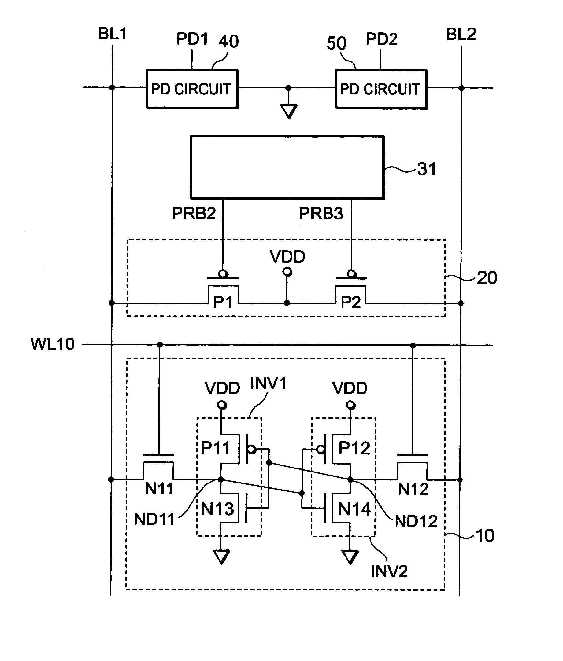
[0060]FIG. 7 is a diagram showing a part of a configuration of the SRAM in a second exemplary embodiment. In the SRAM in the first exemplary embodiment, at the time of the test mode, the precharge circuit 20 is controlled by the precharge control signal PB1 whose signal level changes at the same timing. Thereby, the bit line pair BL1, BL2 was biased with the power supply voltage VDD, and the data of the abnormal memory cell was forcibly inverted. On the other hand, in the SRAM in the second exemplary embodiment, at the time of the test mode, the precharge transistors P1, P2 are controlled by the respective precharge control signals PB2, PB3 whose signal levels change at different timings.

(Configuration of SRAM)

[0061]Referring to FIG. 7, the SRAM in the second exemplary embodiment includes a precharge control circuit 31 instead of the precharge control circuit 30 in the first exemplary embodiment. In the case of the test mode, the precharge control circu...

third exemplary embodiment

3. Third Exemplary Embodiment

[0069]FIG. 9 is a diagram showing a part of a configuration of the SRAM in a third exemplary embodiment. In the SRAM in the first exemplary embodiment, at the time of the test mode, the precharge circuit 20 is controlled by the precharge control signal PB1 whose signal level changes at the same timing. Thereby, the bit line pair BL1, BL2 was biased with the power supply voltage VDD, and the data of the abnormal memory cell was forcibly inverted. On the other hand, in the SRAM in the third exemplary embodiment, at the time of the test mode, the precharge transistors P1, P2 are controlled by the respective precharge control signals PB4, PB5 whose signal levels change at different timings. Moreover, by decreasing the voltage of one of the node pair using the data that is written in an other memory cell connected to the same bit line pair, the SRAM can be made to be SRAM that has further higher detection sensitivity of the abnormality.

(Configuration of SRAM)...


PUM


Abstract

An SRAM includes a memory cell and a precharge circuit. The precharge circuit precharges a bit line pair with a power supply voltage before writing a data in the memory cell or before reading a data therefrom at a time of a normal mode, and which feeds a power supply voltage to at least a low level data-holding node of a node pair of the memory cell at a time of a read test mode, between time for writing a data in the memory cell and time for reading a data therefrom.

Description

INCORPORATION BY REFERENCE[0001]This application is based upon and claims the benefit of priority from Japanese Patent Application No. 2008-225880 which was filed on Sep. 3, 2008, the disclosure of which is incorporated herein in its entirety by reference.BACKGROUND OF THE INVENTION[0002]1. Field of the Invention[0003]The present invention relates to SRAM and a method for testing the SRAM.[0004]2. Description of Related Art[0005]FIG. 1 is a diagram showing configurations of a memory cell 100 and peripheral circuits in a general complementary metal-oxide semiconductor (CMOS) type SRAM. Referring to FIG. 1, the memory cell 100 include a positive feedback loop (flip-flop) composed of two CMOS inverters INV10, INV20, and two N-channel MOS transistors N110, N120 for controlling connections between bit line pair BL10, BV20 and the inverters INV10, INV20 (hereinafter referred to as selection transistors N110, N120).[0006]In detail, the two inverters INV10, INV20 are connected between a fir...

Claims


Application Information

Patent Timeline
Patent Type & Authority Applications(United States)
IPC IPC(8): G11C29/00G11C7/00G11C5/14
CPCG11C7/12G11C11/41G11C2029/1204G11C11/413G11C29/50G11C11/412
Inventor KOBATAKE, HIROYUKI
Owner RENESAS ELECTRONICS CORP
Why Eureka
Try Eureka