Method for fracturing circular patterns and for manufacturing a semiconductor device

a technology of circular patterns and semiconductor devices, applied in the field of lithography, can solve the problems of increasing the difficulty of manufacturing contacts and vias on the semiconductor device,

Active Publication Date: 2010-03-04
D2S
View PDF24 Cites 43 Cited by
  • Summary
  • Abstract
  • Description
  • Claims
  • Application Information

AI Technical Summary

Problems solved by technology

In semiconductor manufacturing, reliably manufacturing contacts and vias is difficult and important, especially when optical lithography is used to manufacture patterns smaller than 80 nm half pitch, where half pitch is one-half of the minimum contact or via size plus one-half of the minimum required space between contacts or vias.
But with decreasing feature sizes, it has become prohibitively expensive or impractical to create

Method used


Image

  • Method for fracturing circular patterns and for manufacturing a semiconductor device
  • Method for fracturing circular patterns and for manufacturing a semiconductor device
  • Method for fracturing circular patterns and for manufacturing a semiconductor device

Examples


Embodiment Construction

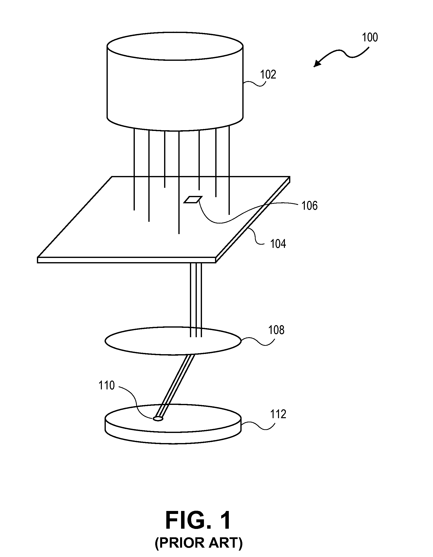
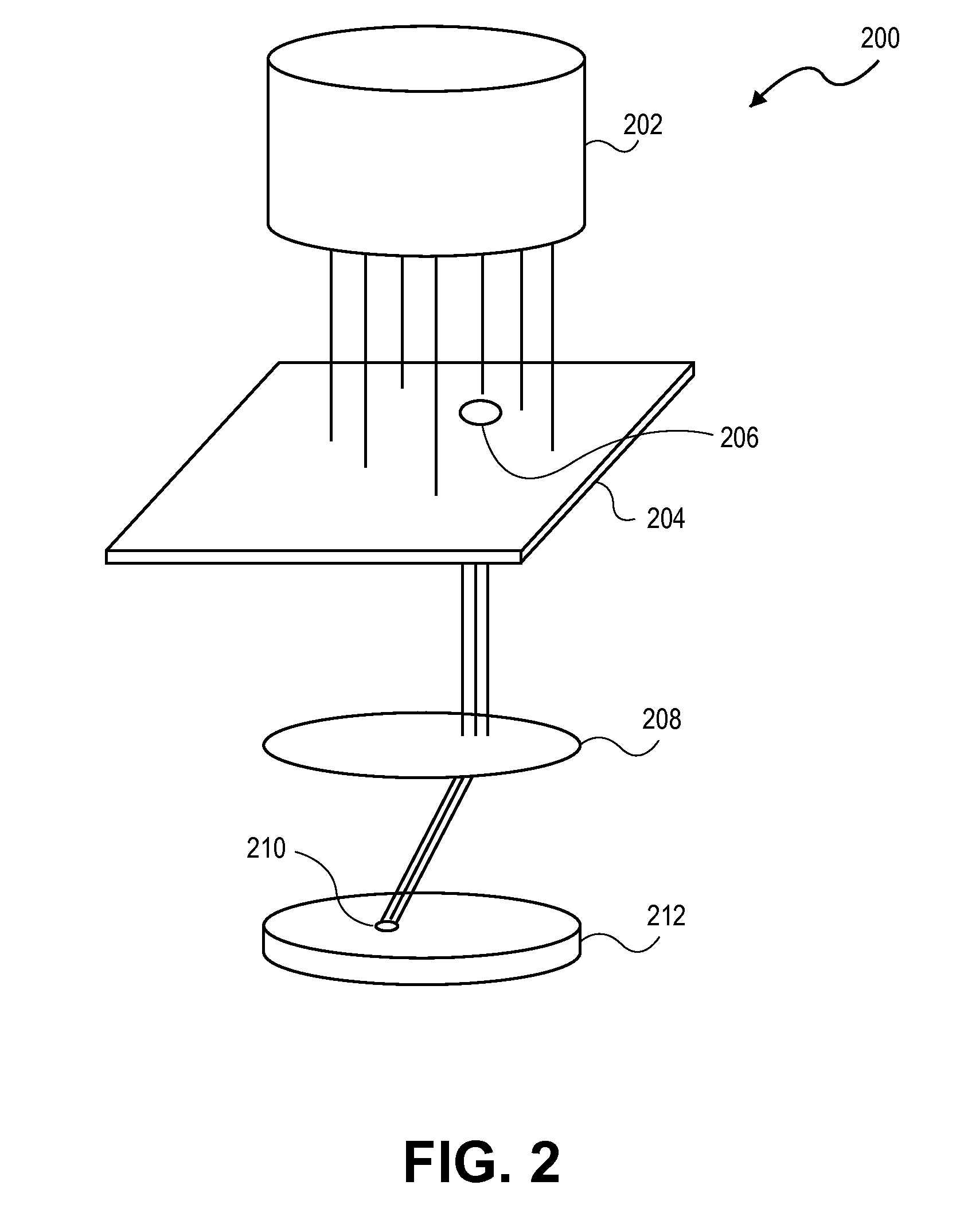
[0023]FIG. 1 illustrates the conventional practice for forming contact and via patterns on a wafer using optical lithography. An optical lithography machine 100 comprises an illumination source 102 which emits optical radiation onto a photomask 104 containing a multiplicity of rectangular aperture patterns 106. Optical radiation is transmitted through the aperture pattern 106 and through one or more lenses 108, thereby forming a pattern 110 on a surface 112, such as a semiconductor wafer. The pattern 110 on the surface 112 is generally reduced in size compared to the aperture pattern 106 on the photomask 104. Due to limitations of the optical lithography process, such as the wavelength of the radiation created by the illumination source 102, for small contact and via patterns, such as for patterns smaller than 80 nm half pitch, the square pattern on the photomask causes a circular or near-circular pattern to be formed on the substrate.

[0024]There is an important concept called Mask ...


PUM


Abstract

A method for manufacturing a semiconductor device using a photomask and optical lithography is disclosed, wherein circular patterns on the semiconductor wafer are formed by using circular patterns on the photomask, which is manufactured using a charged particle beam writer. In one embodiment, circular patterns of varying sizes have been formed on the photomask using a single character projection (CP) character, by varying the charged particle beam dosage. A method for fracturing circular patterns is also disclosed, either using circular CP characters or using VSB shots wherein the union of the plurality of VSB shots is different than the set of desired patterns.

Description

RELATED APPLICATIONS[0001]This application: 1) is a continuation-in-part of U.S. patent application Ser. No. 12 / 202,364 filed Sep. 1, 2008, entitled “Method and System For Manufacturing a Reticle Using Character Projection Particle Beam Lithography”; 2) is a continuation-in-part of U.S. patent application Ser. No. 12 / 473,241 filed May 27, 2009, entitled “Method for Manufacturing a Surface and Integrated Circuit Using Variable Shaped Beam Lithography”; 3) claims priority from U.S. Provisional Patent Application Ser. No. 61 / 224,849 filed Jul. 10, 2009, entitled “Method and System for Manufacturing Circular Patterns On a Surface And Integrated Circuit”; and 4) is related to Fujimura, U.S. patent application Ser. No. ______, entitled “Method and System For Forming Circular Patterns on a Surface” (Attorney Docket No. D2SiP018b) filed on even date herewith; all of which are hereby incorporated by reference for all purposes.BACKGROUND OF THE DISCLOSURE[0002]The present disclosure is relate...

Claims


Application Information

Patent Timeline
IPC IPC(8): G03F7/20G03F1/00
CPCB82Y10/00B82Y40/00H01J37/3174G03F7/2037G03F7/2063G03F1/78G03F1/68Y10S430/143
Inventor FUJIMURA, AKIRATUCKER, MICHAEL
Owner D2S
Why Eureka
Try Eureka