Back contact solar cells using printed dielectric barrier

a dielectric barrier and solar cell technology, applied in the field of photovoltaic cell fabrication, can solve the problems of prior manufacturing methods and add to the cost of solar cell completion

Inactive Publication Date: 2010-03-04
APPLIED MATERIALS INC
View PDF99 Cites 97 Cited by
  • Summary
  • Abstract
  • Description
  • Claims
  • Application Information

AI Technical Summary

Problems solved by technology

However, there are several issues with these prior manufacturing methods.
For example, the formation processes are complicated multistep processes that add to costs required to complete the solar cells.

Method used


Image

  • Back contact solar cells using printed dielectric barrier
  • Back contact solar cells using printed dielectric barrier
  • Back contact solar cells using printed dielectric barrier

Examples


Embodiment Construction

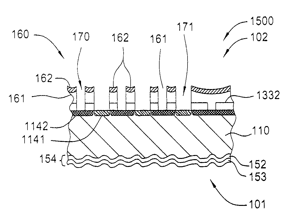
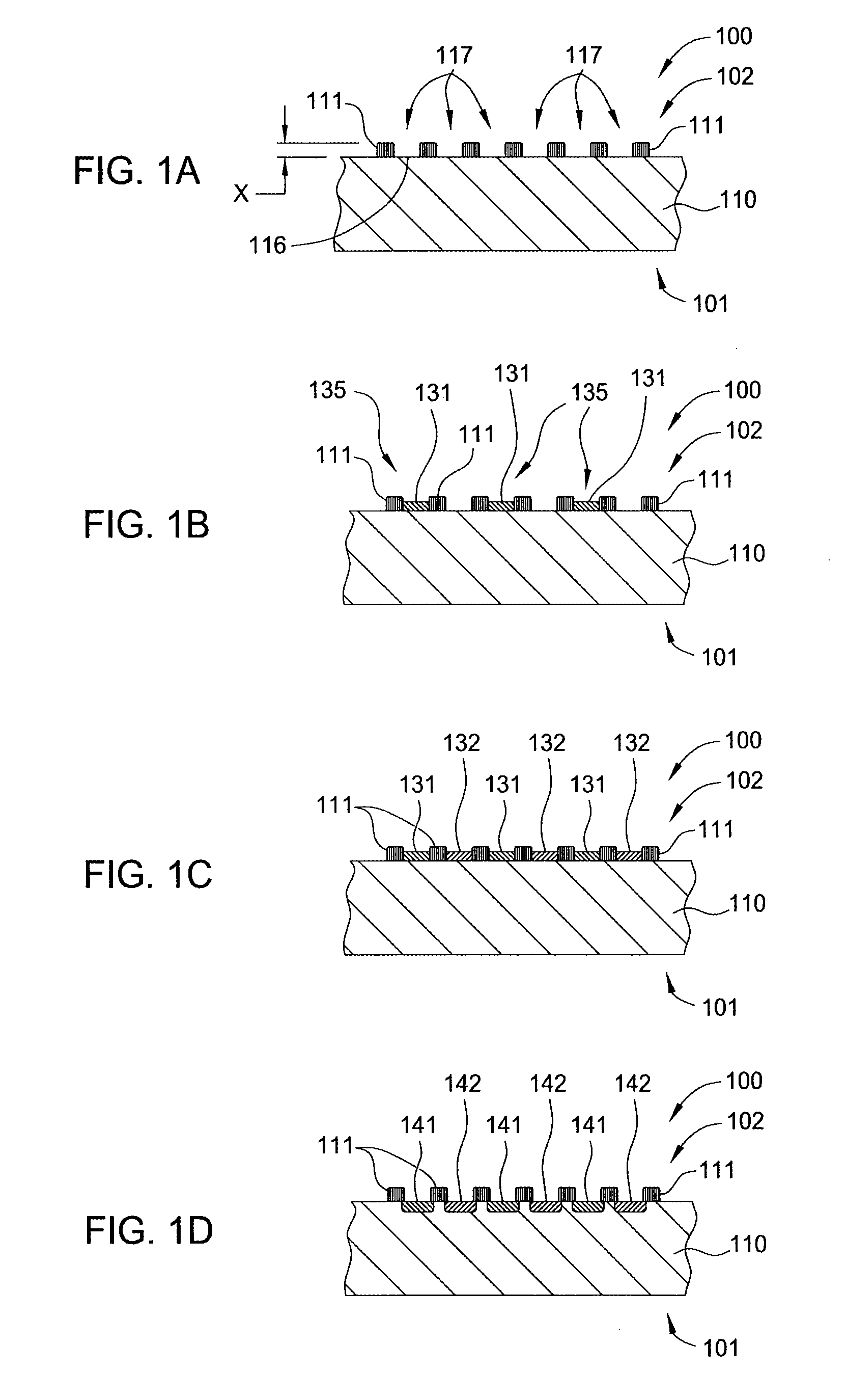
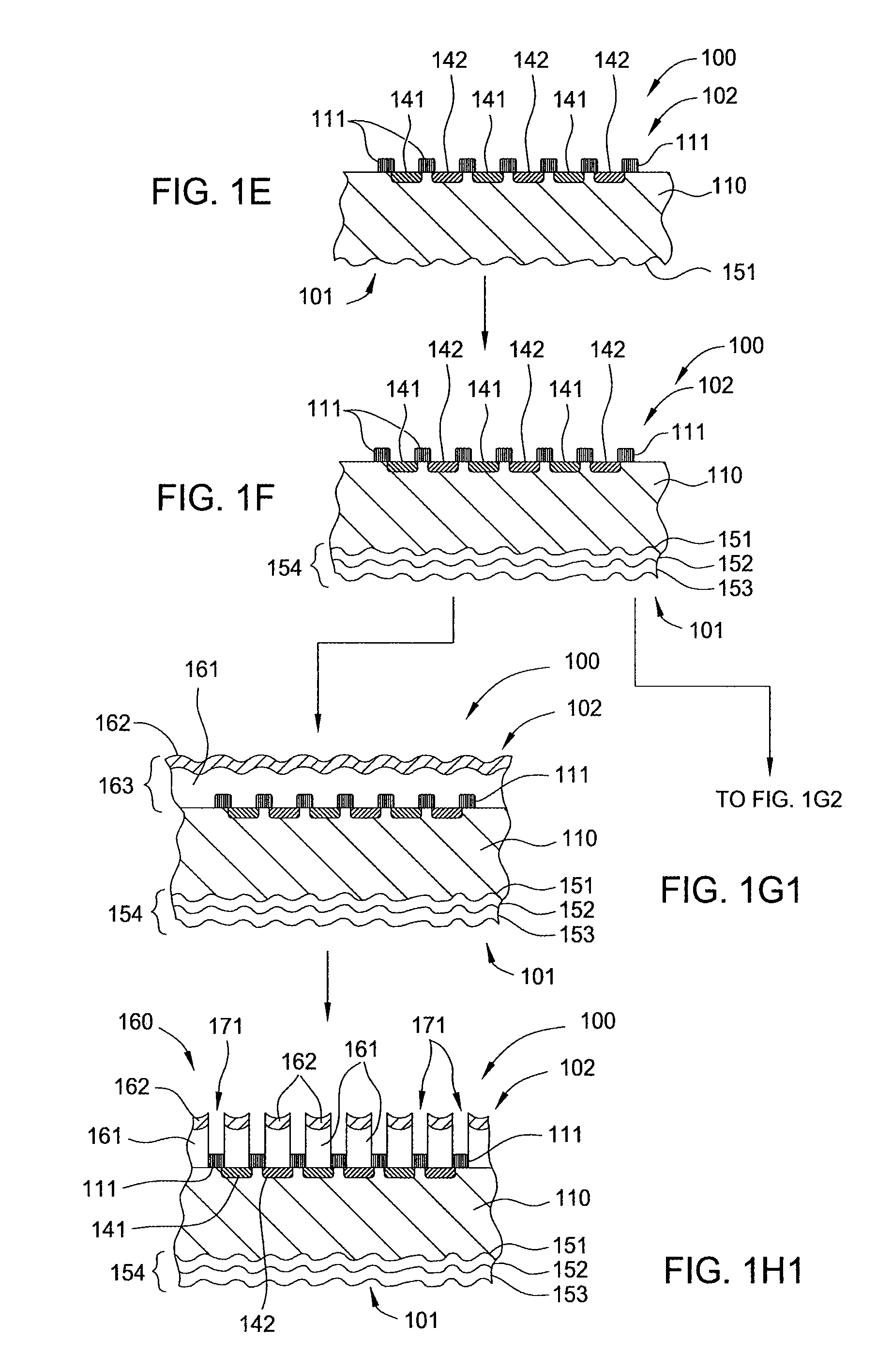
[0041]Embodiments of the invention contemplate the formation of a high efficiency solar cell using novel methods to form the active region(s) and the metal contact structure of a solar cell device. In one embodiment, the methods include depositing a patterned dielectric material that is used to define the active regions and / or contact structure of a solar cell device. Various techniques may be used to form the active regions of the solar cell and the metal contact structure. Solar cell substrates (e.g., substrate 110 in FIG. 1A) that may benefit from the invention include substrates that may have an active region that contains organic material, single crystal silicon, multi-crystalline silicon, polycrystalline silicon, germanium (Ge), gallium arsenide (GaAs), cadmium telluride (CdTe), cadmium sulfide (CdS), copper indium gallium selenide (CIGS), copper indium selenide (CuInSe2), gallium indium phosphide (GaInP2), as well as heterojunction cells, such as GaInP / GaAs / Ge or ZnSe / GaAs / Ge...


PUM

PropertyMeasurementUnit
temperaturesaaaaaaaaaa

Abstract

Embodiments of the invention contemplate the formation of a high efficiency solar cell using novel methods to form the active doped region(s) and the metal contact structure of the solar cell device. In one embodiment, the methods include the steps of depositing a dielectric material that is used to define the boundaries of the active regions and / or contact structure of a solar cell device. Various techniques may be used to form the active regions of the solar cell and the metal contact structure.

Description

CROSS-REFERENCE TO RELATED APPLICATIONS[0001]This application claims benefit of U.S. Provisional Application Ser. No. 61 / 092,379 filed Aug. 27, 2008 (Attorney Docket No. APPM / 13437L) and U.S. Provisional Application Ser. No. 61 / 105,029, filed Oct. 13, 2008 (Attorney Docket No. APPM / 13437L02) and U.S. Provisional Application Ser. No. 61 / 139,423 filed Dec. 19, 2008 (Attorney Docket No. APPM / 13437L03) and U.S. Provisional Application Ser. No. 61 / 157,179 filed Mar. 3, 2009 (Attorney Docket No. APPM / 14258L), all of which are incorporated by references in their entirety.BACKGROUND OF THE INVENTION[0002]1. Field of the Invention[0003]Embodiments of the invention generally relate to the fabrication of photovoltaic cells.[0004]2. Description of the Related Art[0005]Solar cells are photovoltaic devices that convert sunlight directly into electrical power. The most common solar cell material is silicon, which is in the form of single or multicrystalline substrates, sometimes referred to as waf...

Claims


Application Information

Patent Timeline
Patent Type & Authority Applications(United States)
IPC IPC(8): H01L31/18
CPCG01T1/2018H01L21/225H01L21/306H01L21/308H01L21/67034H01L21/67727Y02E10/547H01L21/67745H01L21/6776H01L31/022441H01L31/0516H01L31/0682H01L31/1804H01L21/67736Y02P70/50
Inventor WEIDMAN, TIMOTHY W.MISHRA, ROHITSTEWART, MICHAEL P.WIJEKOON, KAPILA P.CHA, YONGHWA CHRISHOLTAM, TRISTANSHAH, VINAY
Owner APPLIED MATERIALS INC
Why Eureka
Try Eureka