Methods of Fabrication of Solar Cells Using High Power Pulsed Magnetron Sputtering

a technology of solar cells and pulsed magnetron, applied in the field of solar cells, can solve the problems of shunting of solar cells, deterioration of polyimide films commercially available, and difficulty in isolation layer

Inactive Publication Date: 2010-03-04
GENERAL ELECTRIC CO
View PDF8 Cites 55 Cited by
  • Summary
  • Abstract
  • Description
  • Claims
  • Application Information

AI Technical Summary

Benefits of technology

[0006]In accordance with an aspect of the present technique, a method of fabricating a thin-film solar cell is provided. The method includes depositing a transparent conductive contact layer on a surface of a substrate, where the transparent conductive contact layer is configured to act as a front electrode for the solar cell, depositing a window layer over the transparent conductive contact layer, depositing an absorber layer on the window layer, where the absorber layer and the window layer are oppositely doped and form a semiconductor junction, and where at least one of the window layer or the absorber layer is deposited by employing high power pulsed magnetron sputtering, and depositing an electrically conductive film on the semiconductor junction, where the electrically conductive film is configured to act as a back electrode layer for the solar cell.
[0007]In accordance with one aspect of the present technique, a method of fabricating a thin-film solar cell is provided. The method includes depositing a transp...

Problems solved by technology

The drawback of metal foils (e.g., titanium and steel) is that they are electrically conductive, and thus, an electrically isolating layer is needed in order to allow monolithic series-interconnection of the cells.
Such an isolation layer is not easy to make without local defects that may cause shunting of the solar cells.
Further, the polyimide films commercially available deteriorate at temperatures above 400° C. For example, polyimides have high thermal expansion at such high temperatures.
Because subsequent proce...

Method used


Image

  • Methods of Fabrication of Solar Cells Using High Power Pulsed Magnetron Sputtering
  • Methods of Fabrication of Solar Cells Using High Power Pulsed Magnetron Sputtering
  • Methods of Fabrication of Solar Cells Using High Power Pulsed Magnetron Sputtering

Examples


Embodiment Construction

[0016]Embodiments of the present technique provide methods of fabricating diode structures, such as solar cells. The methods employ high power pulsed magnetron sputtering to deposit different layers of the solar cells. As will be described in detail below, in some embodiments, all or some of the layers of the solar cells may be deposited using the high power pulsed magnetron sputtering.

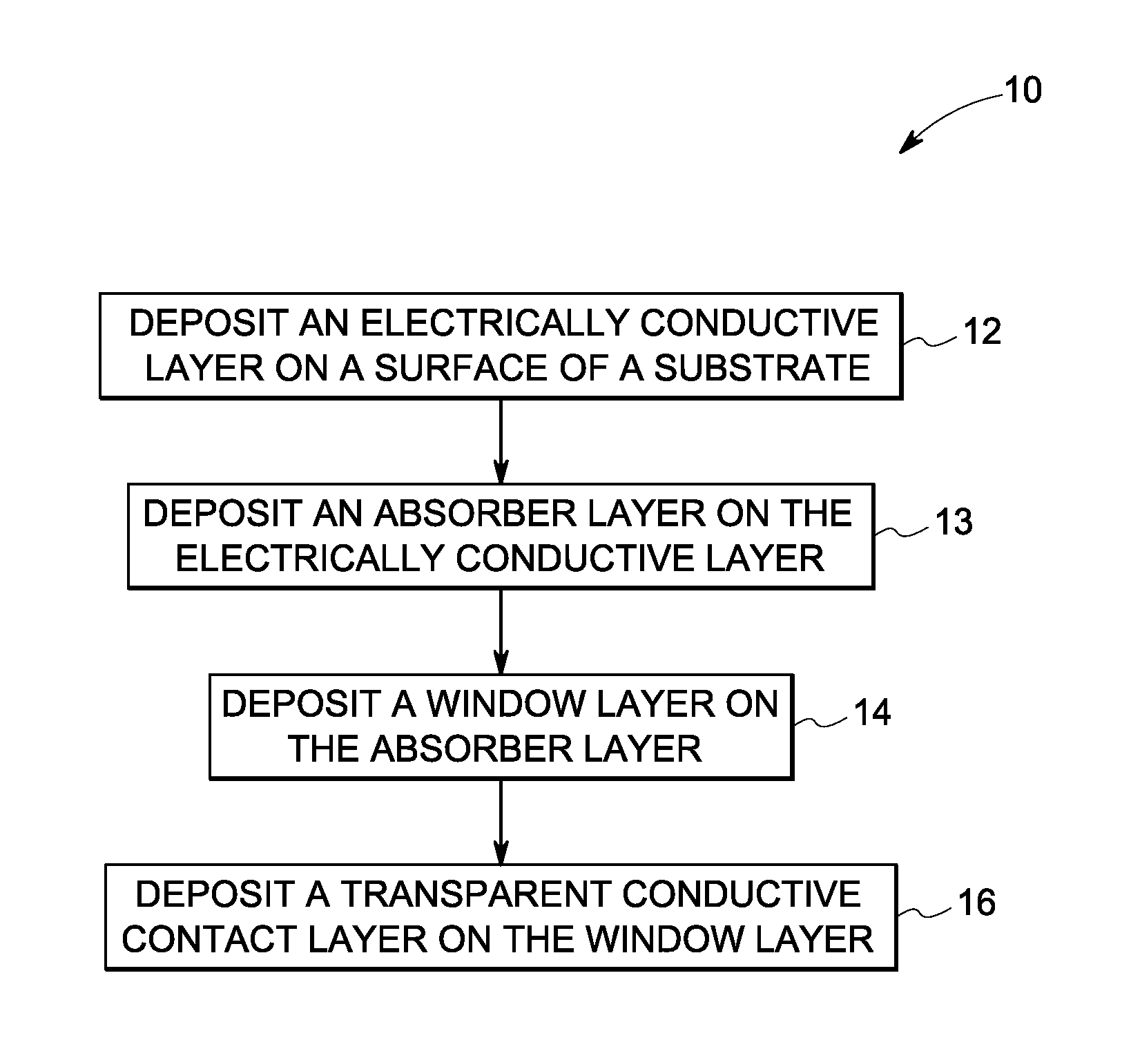
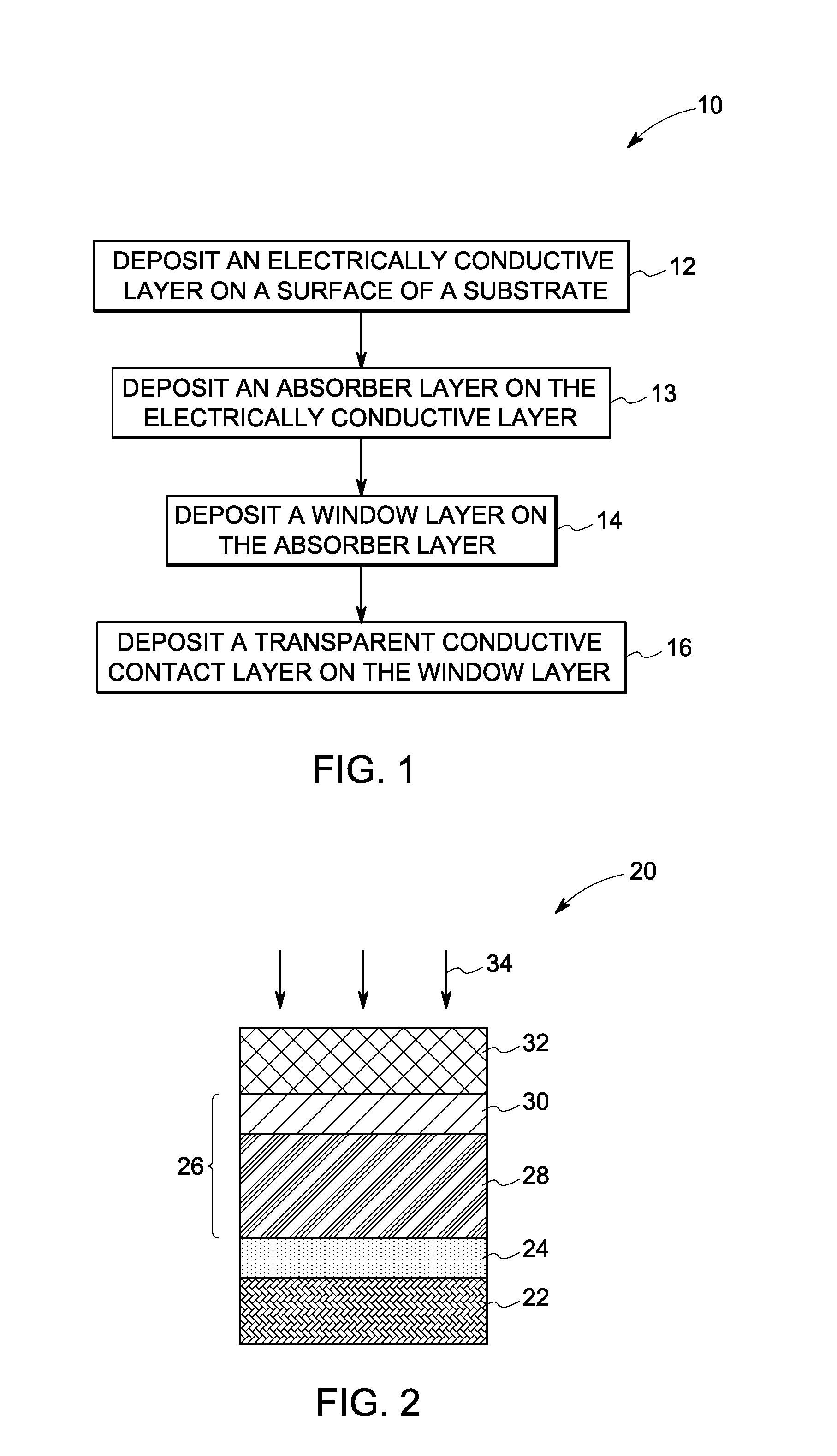
[0017]As illustrated in FIG. 1, a flow chart 10 illustrates a method of fabricating a solar cell. The method includes depositing an electrically conductive layer on a surface of a substrate (block 12). The electrically conductive layer provides ohmic contact to the solar cell. Although not illustrated, the electrically conductive layer may contain one or more layers. For example, the electrically conductive layer may contain a dual layer structure, where one layer provides stable contact with the semiconductor junction, and the other layer provides electrical conductivity. At block 13, an absorber lay...


PUM

PropertyMeasurementUnit
Fractionaaaaaaaaaa
Timeaaaaaaaaaa
Timeaaaaaaaaaa

Abstract

A method of fabricating a solar cell is provided. The method includes depositing a transparent conductive contact layer on a surface of a substrate, where the transparent conductive contact layer is configured to act as a front electrode for the solar cell, depositing a window layer over the transparent conductive contact layer, depositing an absorber layer on the window layer, wherein the absorber layer and the window layer are oppositely doped and form a semiconductor junction, and where at least one of the window layer or the absorber layer is deposited by employing high power pulsed magnetron sputtering, and depositing an electrically conductive film on the semiconductor junction, wherein the electrically conductive film is configured to act as a back electrode layer for the solar cell.

Description

BACKGROUND[0001]The invention relates generally to the field of solar cells, and more particularly to methods of fabrication of solar cells.[0002]Solar cells are used for converting solar energy into electrical energy. Typically, in its basic form, a solar cell includes a semiconductor junction made of two or three layers that are disposed on a substrate layer, and two contacts (electrically conductive layers) for passing electrical energy in the form of electrical current to an external circuit.[0003]Thin-film solar cells have a great potential for cost reduction because they require only a small amount of materials deposited directly on large area substrates, and their manufacture is suited to fully integrated processing and high throughputs. Alternatives for substrate materials that can be employed in solar cells include glass, titanium, steel, or polyimide. The drawback of metal foils (e.g., titanium and steel) is that they are electrically conductive, and thus, an electrically ...

Claims


Application Information

Patent Timeline
IPC IPC(8): H01L21/00
CPCC23C14/0629C23C14/086C23C14/3485C23C14/35H01L21/02439H01L21/02551Y02E10/541H01L21/02631H01L31/0322H01L31/0324H01L31/0749H01L31/1836H01L21/02568
Inventor ZHONG, DALONGJOHNSON, JAMES NEILZHANG, XIAOLAN
Owner GENERAL ELECTRIC CO
Why Eureka
Try Eureka