This helps you quickly interpret patents by identifying the three key elements:
Problems solved by technology
Method used
Benefits of technology
Benefits of technology
[0018]According to an embodiment of the present invention, even when an SOI substrate in which a semiconductor film is formed over a glass substrate is used, a conductive film, the semiconductor film, and an insulating film are prevented from being peeled by stress that the conductive film has, in formation of the conductive film used as a gate electrode. In addition, formation of a wiring pattern is not disturbed by particles of the peeled conductive film, insulating film, and semiconductor film. Therefore, a semiconductor device which has high reliability sufficient for practical use can be manufactured. Furthermore, reduction in yield due to peeling of the conductive film, the semiconductor film, and the insulating film during manufacture of a semiconductor device can be prevented.
Problems solved by technology
Particles of the peeled conductive film, insulating film, and semiconductor film cause electrical short circuit between regions of wirings which should be separated, separation of portions which should be electrically connected, and the like and disturb formation of a wiring pattern.
Method used
Image
Click on the blue label to locate the original text in one second.
Reading with bidirectional positioning of images and text.
Examples
embodiment 1
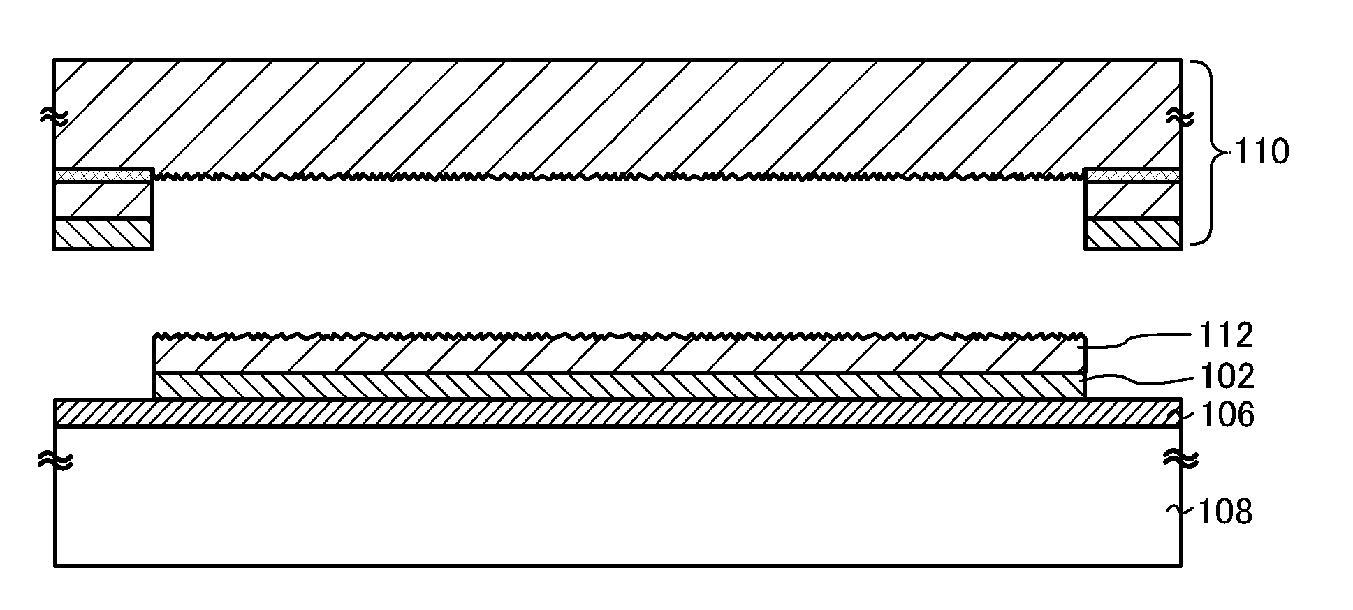
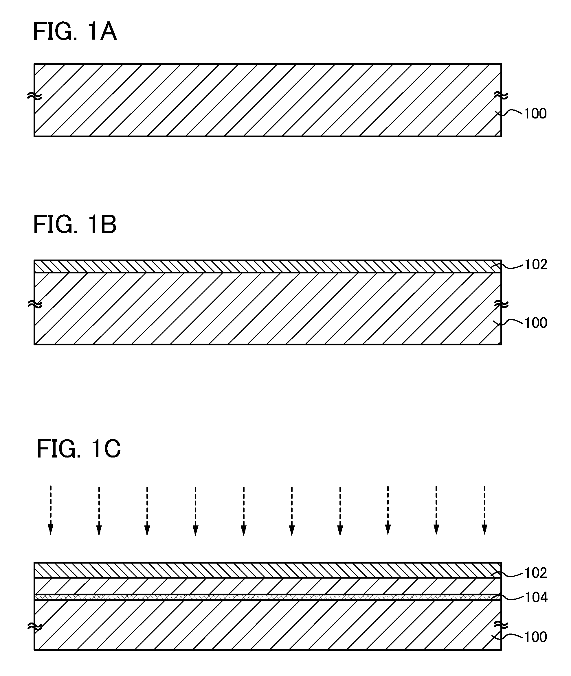
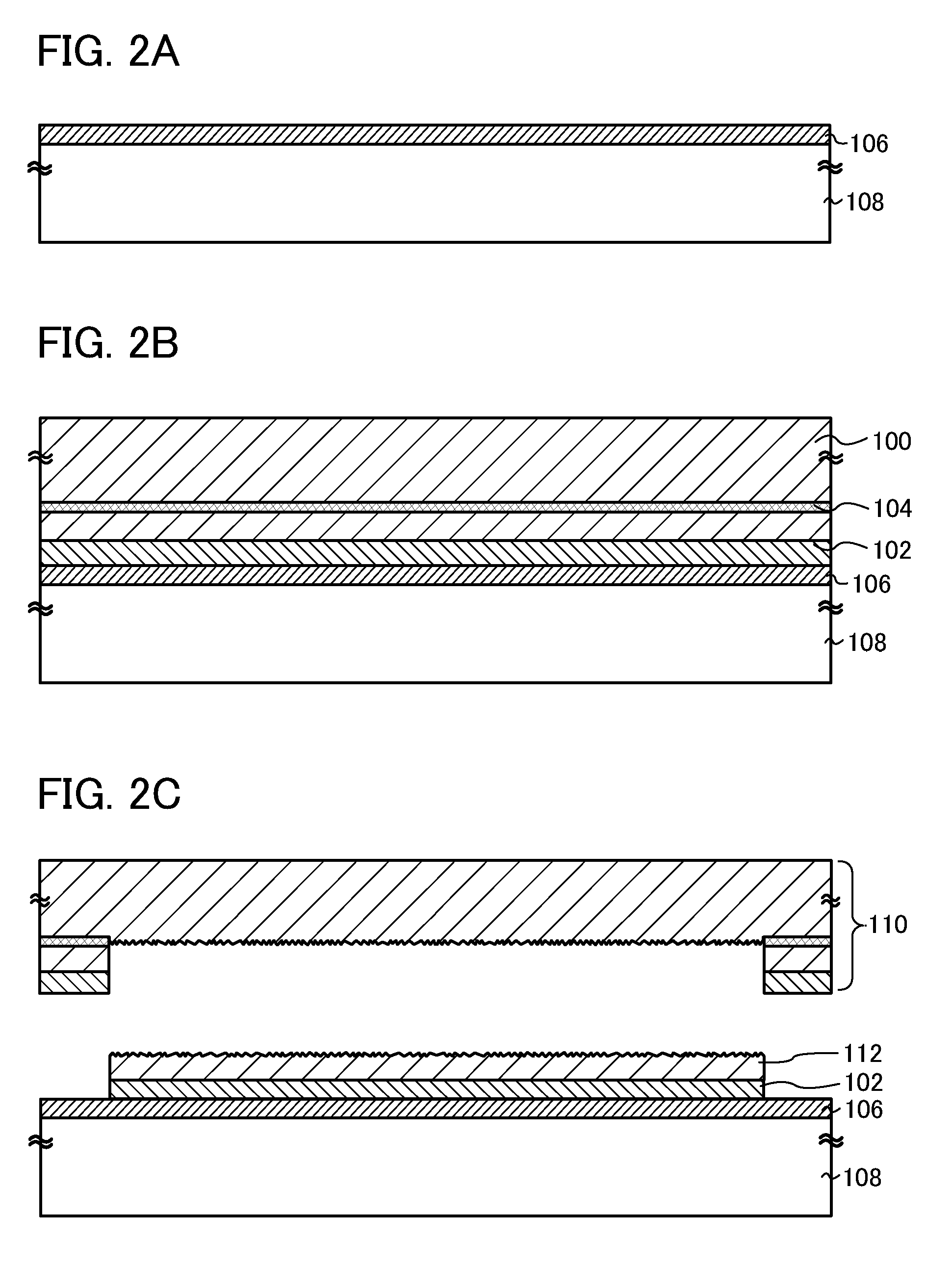
[0038]In a manufacturing method of a semiconductor device according to Embodiment 1, an SOI substrate is manufactured in such a manner that a semiconductor film separated from a semiconductor substrate which is a bond substrate is bonded to a base substrate. Then, with the use of the manufactured SOI substrate, a semiconductor device is manufactured. A manufacturing method of a semiconductor device according to this embodiment will be described below with reference to FIGS. 1A to 1C, FIGS. 2A to 2C, FIGS. 3A to 3C, FIGS. 4A to 4D, FIGS. 5A to 5C, FIGS. 6A to 6C, and FIGS. 8A to 8C.
[0039]First, a bond substrate 100 as illustrated in FIG. 1A is prepared. As the bond substrate 100, a commercial semiconductor substrate can be used; for example, a single crystal semiconductor substrate or a polycrystalline semiconductor substrate of silicon, germanium, or the like can be used. In addition, a single crystal semiconductor substrate or a polycrystalline semiconductor substrate formed of a c...
embodiment 2
[0150]In Embodiment 2, a manufacturing method of a semiconductor device in which sidewalls are formed differently from Embodiment 1 to form high-concentration impurity regions, low-concentration impurity regions, and a channel formation region in a semiconductor film will be described with reference to FIGS. 7A to 7D.
[0151]First, in a similar manner to that of Embodiment 1, the insulating film 106, the insulating film 102, the semiconductor film 116, and the semiconductor film 118 are formed over the glass substrate 108 and they are covered with the gate insulating film 120, the first conductive film 122, and the second conductive film 124 as illustrated in FIG. 4C.
[0152]Next, the resistmask 126 and the resistmask 128 are selectively formed over the second conductive film 124. Then, the first conductive film 122 and the second conductive film 124 are etched using the resistmask 126 and the resist mask 128. Accordingly, a gate electrode 208 with a two-layer structure formed of a f...
embodiment 3
[0159]In Embodiment 3, a specific mode of a semiconductor device manufactured by application of an embodiment of the present invention will be described with reference to FIG. 9 and FIG. 10.
[0160]First, a microprocessor will be described as an example of a semiconductor device. FIG. 9 is a block diagram illustrating a structural example of a microprocessor 500.
[0161]The microprocessor 500 includes an arithmetic logic unit (also referred to as an ALU) 501, an ALU controller 502, an instruction decoder 503, an interrupt controller 504, a timing controller 505, a register 506, a register controller 507, a bus interface (Bus I / F) 508, a read-only memory (ROM) 509, and a ROM interface (ROM I / F) 510.
[0162]An instruction input to the microprocessor 500 through the bus interface 508 is input to the instruction decoder 503 and decoded. Then, the instruction is input to the ALU controller 502, the interrupt controller 504, the register controller 507, and the timing controller 505. The ALU co...
PUM
Abstract
To provide a manufacturing method of a semiconductor device in which, even when the semiconductor device is formed over an SOI substrate which uses a glass substrate, an insulating film and a semiconductor film over the glass substrate are not peeled by stress applied by a conductive film in formation of the conductive film for forming a gate electrode. A semiconductor device is manufactured by the steps of forming a first insulating film over a bond substrate, forming an embrittlement layer by adding ions from a surface of the bond substrate, bonding the bond substrate to a glass substrate with the first insulating film interposed therebetween, separating the bond substrate along the embrittlement layer to form a semiconductor film over the glass substrate with the first insulating film interposed therebetween, removing a peripheral region of the first insulating film and the semiconductor film to expose part of the glass substrate, forming a gate insulating film over and in contact with the semiconductor film and the glass substrate, and forming a stacked conductive film over and in contact with the gate insulating film, in which the stacked conductive film includes a conductive film having a tensile stress and a conductive film having a compressive stress.
Description
BACKGROUND OF THE INVENTION[0001]1. Field of the Invention[0002]The present invention relates to a manufacturing method of a semiconductor device that uses a substrate provided with a semiconductor layer with an insulating film interposed therebetween, in particular, an SOI (silicon on insulator) substrate.[0003]2. Description of the Related Art[0004]In recent years, integrated circuits that use an SOI (silicon on insulator) substrate in which a thin single crystal semiconductor layer is provided on an insulating surface, instead of a bulk siliconwafer, have been developed. By utilizing characteristics of a thin single crystal silicon film formed over an insulating film, transistors formed in the integrated circuit can be separated from each other completely. Further, since fully-depleted transistors can be formed, a semiconductor integrated circuit with high added value such as high integration, high speed driving, and low power consumption can be realized.[0005]As one of the meth...
Claims
Application Information
Patent Timeline
Application Date:The date an application was filed.
Publication Date:The date a patent or application was officially published.
First Publication Date:The earliest publication date of a patent with the same application number.
Issue Date:Publication date of the patent grant document.
PCT Entry Date:The Entry date of PCT National Phase.
Estimated Expiry Date:The statutory expiry date of a patent right according to the Patent Law, and it is the longest term of protection that the patent right can achieve without the termination of the patent right due to other reasons(Term extension factor has been taken into account ).
Invalid Date:Actual expiry date is based on effective date or publication date of legal transaction data of invalid patent.

