Method for forming gate spacers for semiconductor devices

Inactive Publication Date: 2010-03-11
TOKYO ELECTRON LTD
View PDF11 Cites 54 Cited by
  • Summary
  • Abstract
  • Description
  • Claims
  • Application Information

AI Technical Summary

Benefits of technology

[0004]Embodiments of the invention provide a method for integrating formation of gate spacers around patterned gate structures into semiconductor manufacturing. The method prevents or minimizes formation of an oxidized gate electrode region that can increase in the equivalent oxide thickness (EOT) of the patterned gate structure and changes in the effective workfunction of the patterned gate structure near the source/drain regions.
[0005]According to one embodiment of the invention, the method includes forming a patterned gate structure on a substrate, the patterned gate structure containing an interface layer on the substrate, a high-k film on the interface layer, and a gate electrode on the high-k film. The method further includes depositing a nitride barrier layer on the patterned gate structure in a process chamber using processing con

Problems solved by technology

Formation of a conventional gate spacer around a patterned gate structure frequently results in unwanted oxidation of the patterned gate structure that can affect device performance.
For example, oxidation of the sidewalls of the patterned gate structure in

Method used


Image

  • Method for forming gate spacers for semiconductor devices
  • Method for forming gate spacers for semiconductor devices
  • Method for forming gate spacers for semiconductor devices

Examples


Embodiment Construction

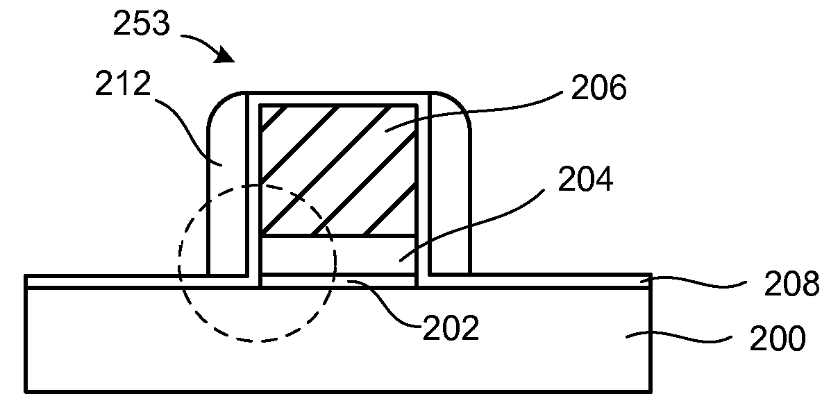
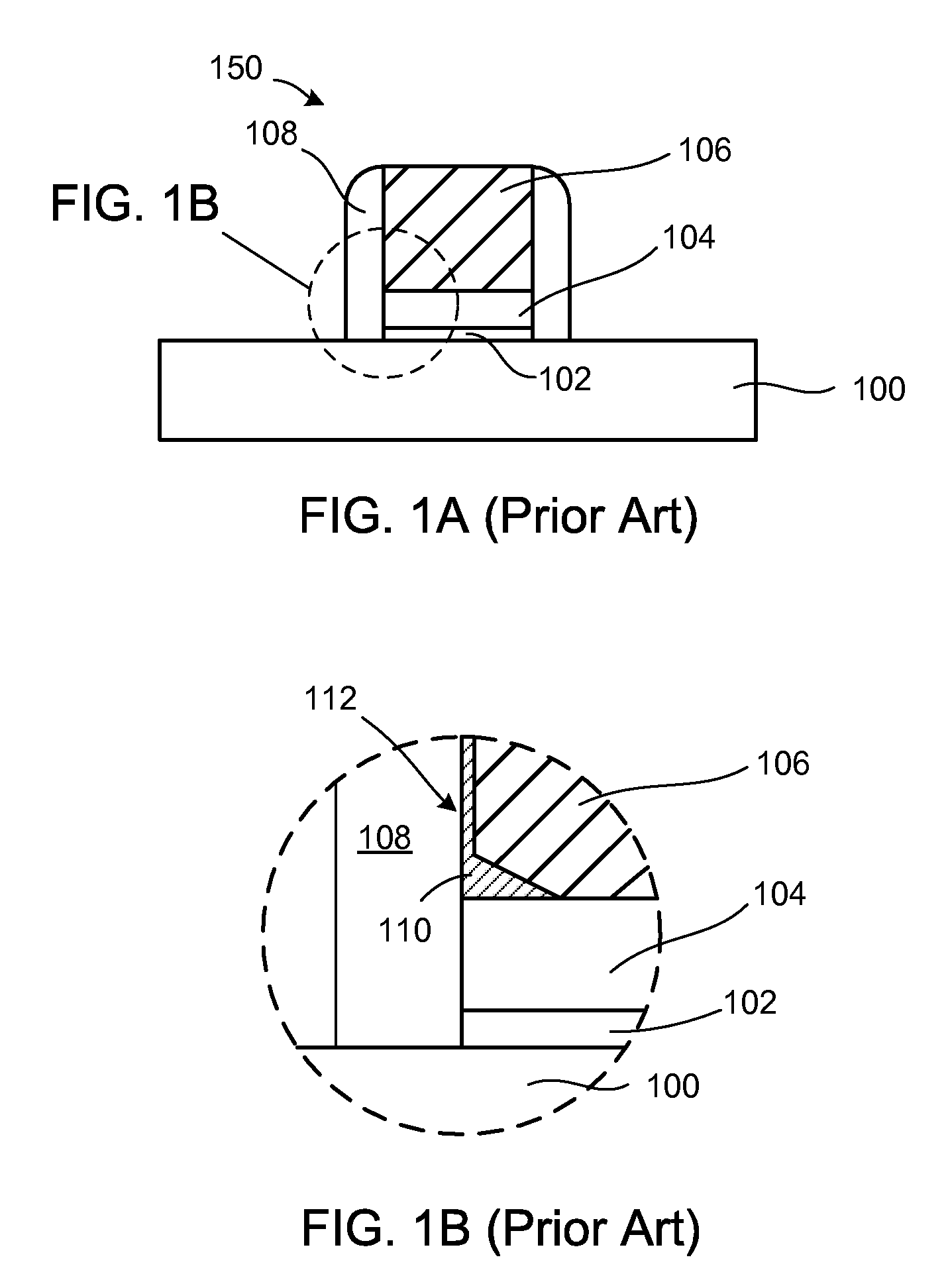
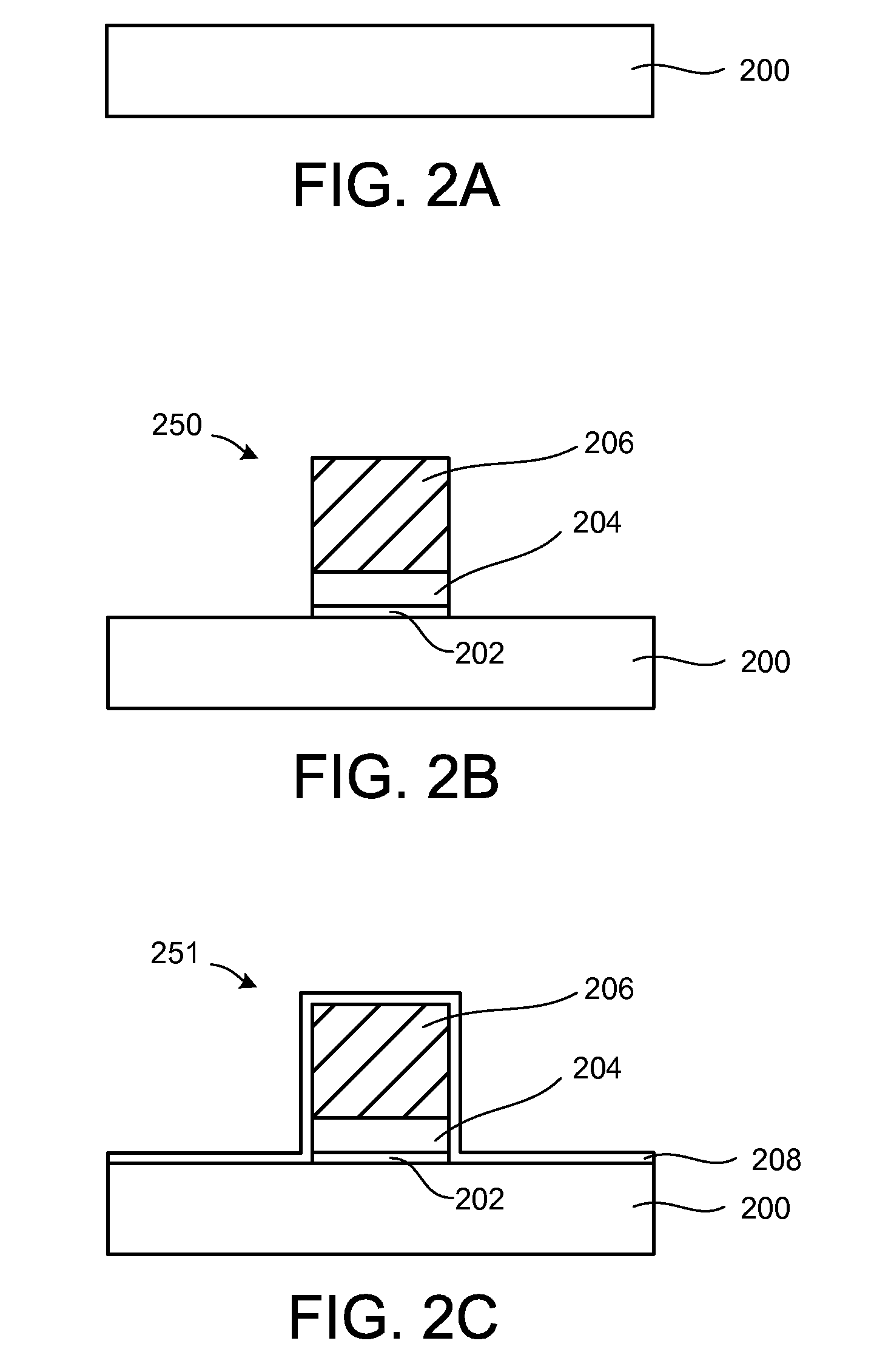
[0014]Methods for forming patterned gate structures containing a gate spacer for semiconductor devices are disclosed in various embodiments. However, one skilled in the relevant art will recognize that the various embodiments may be practiced without one or more of the specific details, or with other replacement and / or additional methods, materials, or components. In other instances, well-known structures, materials, or operations are not shown or described in detail to avoid obscuring aspects of various embodiments of the invention. Similarly, for purposes of explanation, specific numbers, materials, and configurations are set forth in order to provide a thorough understanding of the invention. Furthermore, it is understood that the various embodiments shown in the drawings are illustrative representations and are not necessarily drawn to scale.

[0015]Reference throughout this specification to “one embodiment” or “an embodiment” means that a particular feature, structure, material, ...


PUM


Abstract

A method for forming gate spacers for semiconductor devices includes forming a patterned gate structure on substrate, where the patterned gate structure contains an interface layer on the substrate, a high-k film on the interface layer, and a gate electrode on the high-k film. The method further includes depositing a nitride barrier layer on the patterned gate structure using processing conditions that minimize or prevent oxidation of the substrate and the gate electrode, depositing a spacer material on the nitride barrier layer, and anisotropically etching the spacer material to form a gate spacer on the patterned gate structure.

Description

FIELD OF INVENTION[0001]The present invention relates generally to the field of fabrication of semiconductor devices, and more particularly, to a method for fabricating a gate spacer on a sidewall of a patterned gate structure of a semiconductor device.BACKGROUND OF THE INVENTION[0002]In the semiconductor industry, the minimum feature sizes of microelectronic devices are approaching the deep sub-micron regime to meet the demand for faster, lower power microprocessors and digital circuits. Metal oxide semiconductor field effect transistors (MOSFETs) have been continuously scaled down to gain improved device density, operating performance, and reduced fabrication cost for integrated circuits (ICs).[0003]A gate spacer formed around a patterned gate structure of a MOSFET is typically used as an implant mask in a self aligned drain and source implantation. In addition, the gate spacer is used to isolate drain / source electrodes from a patterned gate structure when the drain / source electro...

Claims


Application Information

Patent Timeline
IPC IPC(8): H01L21/3205
CPCH01L21/28176H01L21/67184H01L29/6656H01L29/51H01L21/67207
Inventor CLARK, ROBERT D.
Owner TOKYO ELECTRON LTD
Why Eureka
Try Eureka