Wide wave apparatus for soldering an electronic assembly

a technology of electronic assembly and wave wave, which is applied in the direction of soldering apparatus, manufacturing tools, solder feeding devices, etc., can solve the problems of increasing the complexity of the product to be wave soldered, the difficulty of current wave soldering machines and processes in overcoming the fundamental lead-free alloy attributes, and the inability to meet the requirements of wave soldering, etc., to achieve the effect of improving the wave soldering capability, reducing defects, and improving throughput speed

Inactive Publication Date: 2010-03-18
SZYMANOWSKI RICHARD ANTHONY
View PDF9 Cites 16 Cited by
  • Summary
  • Abstract
  • Description
  • Claims
  • Application Information

AI Technical Summary

Benefits of technology

[0016]The invention provides a wave soldering system that will allow faster throughput speeds and lower defects when wave soldering, especially with lead free solder. It will improve the wave solder capability to manufacture the newer and more challenging product designs. It is equally effective with traditional tin-lead solder alloys.
[0017]The innovation and value of the invention goes directly to the first solder nozzle form. The most significant attributes of the invention are the optimization of the soldering flux used in the process, and superior solder flow dynamics, both of which contribute to correcting the lead-free solder problems of un-filled solder joints and reduced machine through-put.
[0018]Instead of the traditional first solder nozzle that is a narrow solder wave form that was not designed to solder TH

Problems solved by technology

In recent years, two significant changes have taken place, making the above process less efficient, more expensive and, in many cases, inadequate.
Second, the product to be wave soldered has become more complicated and the demand for quality and cost improvement have been emphasized.
With lead-free soldering, current art wave solder machines and processes have difficulty in overcoming the fundamental lead-free alloy attributes of a higher melting temperature and slower wetting speeds.
These attributes are the root cause problems to all the issues noted.
These alloy limitations cannot be addressed simply with a different soldering flux or higher temperatures, because the electrical assemblies cannot survive those conditions.
While a logical solution would be to design more compatible PWBA, the industry has actually emphasized the opposite, creating new products that are more difficult to solder in any manner.
In current art, especially in lead-free soldering, a leading defect is the inability to achieve fully formed solder joints on the entire assembly, with either one or two solder nozzles being used.
Associated problems affect cost, productivity and quality.
In curr

Method used


Image

  • Wide wave apparatus for soldering an electronic assembly
  • Wide wave apparatus for soldering an electronic assembly
  • Wide wave apparatus for soldering an electronic assembly

Examples


Embodiment Construction

[0028]This invention is not limited in its application to the details of construction and the arrangement of components set forth in the following description or illustrated in the drawings. The invention is capable of other embodiments and of being practiced or of being carried out in various ways. Also, the phraseology and terminology used herein is for the purpose of description and should not be regarded as limiting. The use of “including,”“comprising,”“having,”“containing,”“involving,” and variations thereof herein, is meant to encompass the items listed thereafter and equivalents thereof as well as additional items.

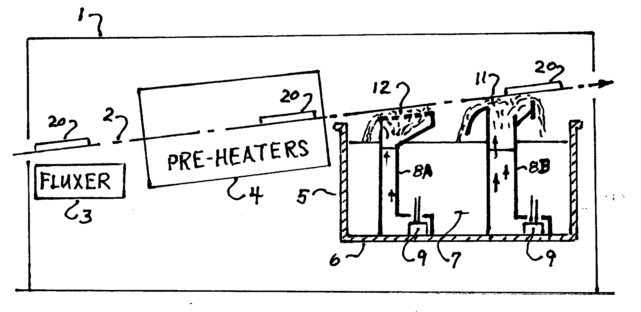
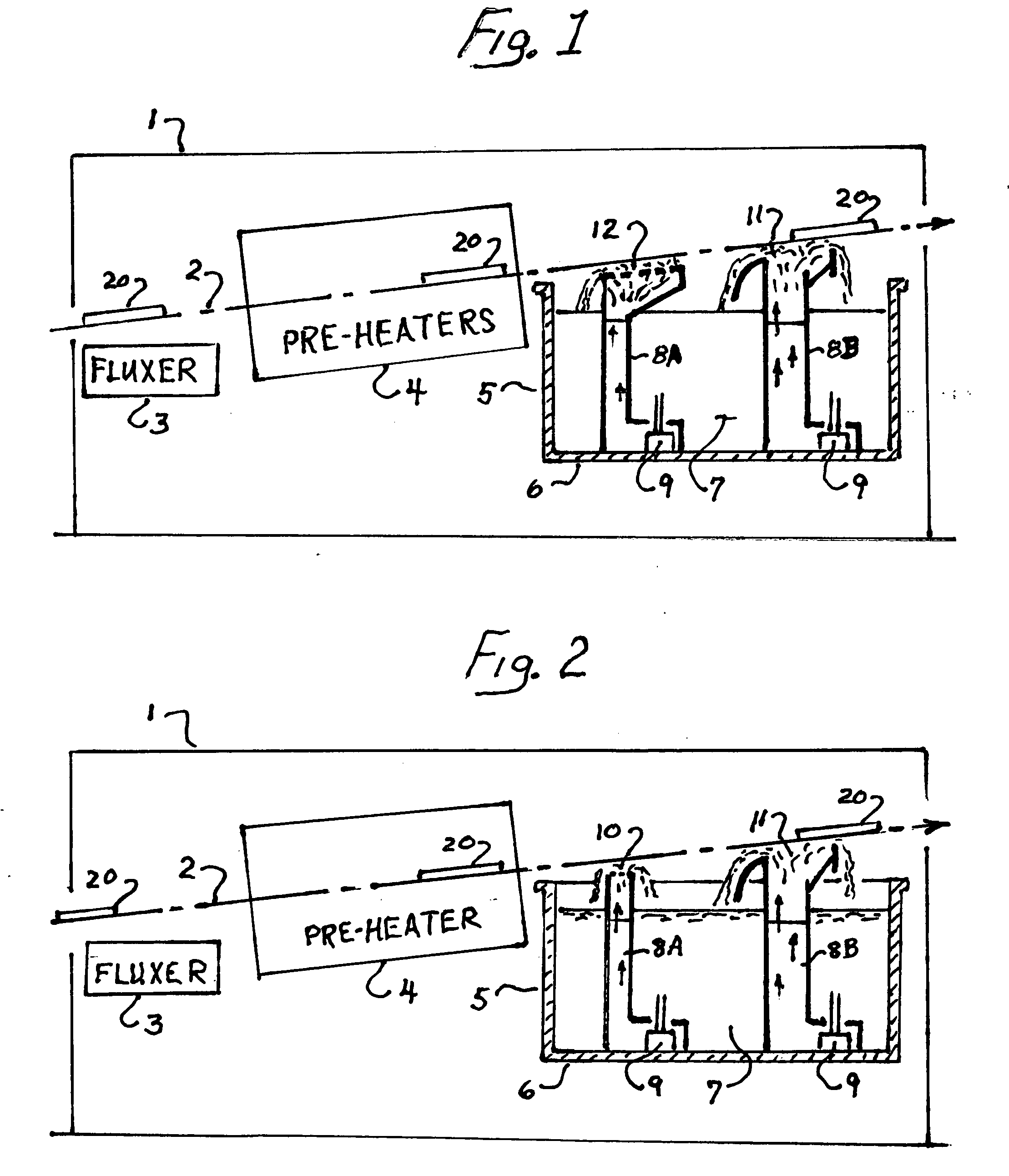
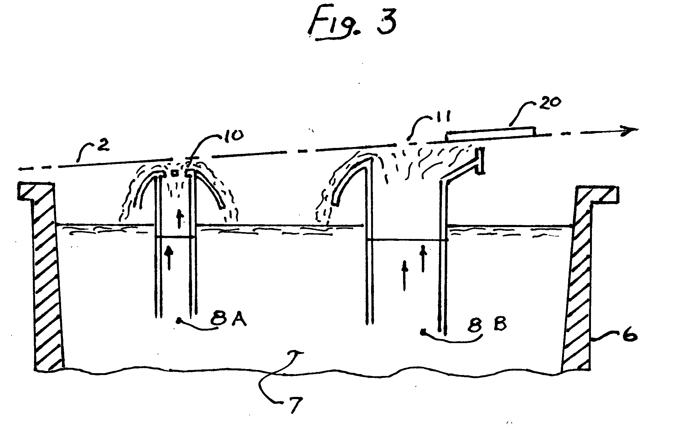
[0029]Starting with FIG. 1 and FIG. 2, the only difference in the wave solder process is by installing the invention 12 as the first solder wave 10 located in the solder pot 6. The machine system 1 is not otherwise affected. Electronic substrate 20 to be soldered, are put on the machine conveyor 2. The conveyor 2 carries the substrate 20 over the flux module 3, thro...


PUM

PropertyMeasurementUnit
Lengthaaaaaaaaaa
Lengthaaaaaaaaaa
Pressureaaaaaaaaaa

Abstract

Especially for but not limited to lead-free solder, the apparatus disclosed herein will provide better quality of wave soldered joints at a lower cost, without the addition of more equipment.
The invention will form complete TH solder joints over the first wave soldering nozzle, not the second wave soldering nozzle which is current art. It specifically addresses the size and the shape of the holes in the first wave-forming nozzle.
The first solder wave forming plate has hexagon shaped holes that reduce the incidence of holes being clogged and non-functional. There is a size gradient across the multiple rows of holes in the extended contact wave former that has the effect of creating a uniform solder pressure across the entire face of the nozzle. The result is higher solder pressure against the electronic substrate being soldered for a longer period of time than current art, allowing for faster formation of solder joints. This affects quality and thru-put.

Description

[0001]Priority for this invention is claimed by virtue of the associated provisional patent application No. 61 / 136,556. The filing date was Sep. 15, 2008. The confirmation number was 7875.BACKGROUND OF INVENTION[0002]1. Field of Invention[0003]This application relates to the general business of electronics manufacturing, and specifically to a common soldering process used in that business. The specific process is called wave soldering and it provides for the mechanical and electrical connection of components to a substrate with molten solder alloy. As a definition of terms, a wave solder machine is a mass soldering machine system, where molten solder is pumped up to form a standing wave, while the product is passed over that wave, thereby forming many solder joints that are uniform, at high efficiency. The machine automatically transports the product across the required process steps to make a solder joint, which includes flux application, pre-heat, and soldering. This application w...

Claims


Application Information

Patent Timeline
IPC IPC(8): B23K3/06B23K1/08
CPCB23K1/0016B23K3/0653B23K1/085
Inventor SZYMANOWSKI, RICHARD ANTHONY
Owner SZYMANOWSKI RICHARD ANTHONY
Why Eureka
Try Eureka